- 您現(xiàn)在的位置:買賣IC網(wǎng) > PDF目錄373714 > TS68230CP10 (意法半導(dǎo)體) HMOS PARALLEL INTERFACE/TIMER PDF資料下載
參數(shù)資料
| 型號(hào): | TS68230CP10 |
| 廠商: | 意法半導(dǎo)體 |
| 英文描述: | HMOS PARALLEL INTERFACE/TIMER |
| 中文描述: | HMO的并行接口/定時(shí)器 |
| 文件頁數(shù): | 26/61頁 |
| 文件大小: | 2911K |
| 代理商: | TS68230CP10 |
第1頁第2頁第3頁第4頁第5頁第6頁第7頁第8頁第9頁第10頁第11頁第12頁第13頁第14頁第15頁第16頁第17頁第18頁第19頁第20頁第21頁第22頁第23頁第24頁第25頁當(dāng)前第26頁第27頁第28頁第29頁第30頁第31頁第32頁第33頁第34頁第35頁第36頁第37頁第38頁第39頁第40頁第41頁第42頁第43頁第44頁第45頁第46頁第47頁第48頁第49頁第50頁第51頁第52頁第53頁第54頁第55頁第56頁第57頁第58頁第59頁第60頁第61頁
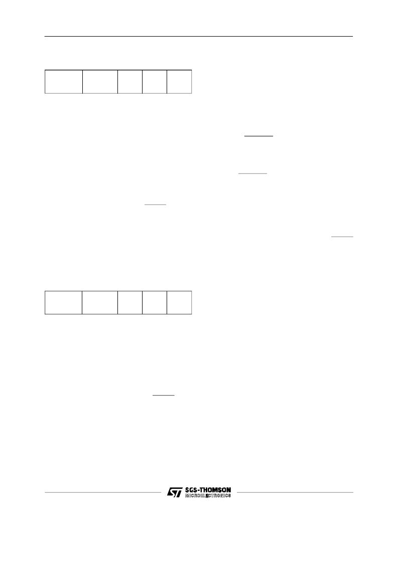
3.4.1. PORT A CONTROL REGISTER (PACR).
The port A control register, in conjunction with the
programmed mode and the port B submode,
controls the operation of port A and the handshake
pins H1 and H2. The port A control register contains
five fields : bits 7 and 6 specify the port A submode ;
bits 5, 4, and 3 control the operation of the H2 hand-
shake pin and H2S status bit ; bit 2 determines whe-
ther an interrupt will be generated when the H2S
status bit goes to one ; bit 1 determines whether a
service request (interrupt request or DMA request)
will occur ; and bit 0 controls the operation of the H1S
status bit. The PACR is always readable and writa-
ble. There is never a consequence to reading the re-
gister.
All bits are cleared to zero when the RESET pin is as-
serted. When the port A submode field is relevant in
a mode/submode definition, it must not be altered un-
less the H12 enable bit in the port general control re-
gister is clear (see table 1.3 located at the end of this
document). Altering these bits may give unpre-
dictable results if the H12 enable bit in the PGCR is
set.
3.4.2. PORT B CONTROL REGISTER (PBCR).
The port B control register specifies the operation of
port B and the handshake pins H3 and H4. The port
B control register contains five fields : bits 7 and 6
specify the port B submode ; bits 5, 4, and 3 control
the operation of the H4 handshake pin and H4S sta-
tus bit goes to a one ; bit 1 determines whether a ser-
vice request (interrupt request or DMA request) will
occur ; and bit 0 controls the operation of the H3S
status bit. The PBCR is always readable and writa-
ble.
All bits are cleared to zero when the RESET pin is
asserted. When the port B submode field is relevant
in a mode/submode definition, it must not be altered
unless the H34 enable bit in the port general control
register is clear (see table 1.3 located at the end of
this document). Altering these bits may give unpre-
dictable results if the H12 enable bit in the PGCR is
set.
3.4.3. SUBMODE X0 - PIN-DEFINABLE DOUBLE-
BUFFERED INPUT OR SINGLE-BUFFERED
OUTPUT. In mode 1 submode X0, double-buffered
input transfers of up to 16 bits may be obtained. The
level of each pin is asynchronously latched with the
asserted edge of H3 and placed in the initial input
latch or the final input latch. The processor may
check the H3S status bit to determine if new data is
present. The DMAREQ pin may be used to signal a
DMA controller to empty the input buffers. Regar-
dless of the bus master, port A data should be read
first and port B data should be read last. The ope-
ration of the internal handshake controller, the H3S
bit, and the DMAREQ are keyed to the reading of the
port B data register. (The 68440 DMAC can be pro-
grammed to perform the exact transfers needed for
compatibility with the PI/T.) H4 may be programmed
as :
1. H4 may be an edge-sensitive status input that
is independent of H3 and the transfer of port
data. On the asserted edge of H4, the H4S sta-
tus bit is set. It is cleared by either the RESET
pin being asserted, writing a one to the parti-
cular status bit in the port status register (PSR),
or when the H34 enable bit of the port general
control register is clear.
2. H4 may be a general-purpose output pin that
is always negated. In this case the H4S status
bit is always clear.
3. H4 may be a general-purpose output pin that
is always asserted. In this case the H4S status
bit is always clear.
4. H4 may be an output pin in the interlocked in-
put handshake protocol. It is asserted when
the port input latches are ready to accept new
data. It is negated asynchronously following
the asserted edge of the H3 input. As soon as
the input latches become ready, H4 is again
asserted. When the input double-buffered
latches are full, H4 remains negated until data
is removed. Thus, anytime the H4 output is as-
serted, new input data may be entered by as-
serting H3. At other times transitions on H3 are
ignored. The H4S status bit is always clear.
When H34 enable in the port general control
register is clear, H4 is held negated.
7
6
5
4
3
2
1
0
Port A
Submode
H2 Control
H2
Interrupt
Enable
H1
SVCRQ
Enable
H1
Status
Control
7
6
5
4
3
2
1
0
Port B
Submode
H4Control
H4
Interrupt
Enable
H3
SVCRQ
Enable
H3
Status
Control
TS68230
26/61
相關(guān)PDF資料 |
PDF描述 |
|---|---|
| TS68230CP8 | HMOS PARALLEL INTERFACE/TIMER |
| TS68230P | HMOS PARALLEL INTERFACE/TIMER |
| TS68230CFN8 | HMOS PARALLEL INTERFACE/TIMER |
| TS68302DESC01QYA | Integrated Multiprotocol Processor IMP |
| TS68302VA16 | Integrated Multiprotocol Processor IMP |
相關(guān)代理商/技術(shù)參數(shù) |
參數(shù)描述 |
|---|---|
| TS68230CP8 | 制造商:STMICROELECTRONICS 制造商全稱:STMicroelectronics 功能描述:HMOS PARALLEL INTERFACE/TIMER |
| TS68230FN | 制造商:STMICROELECTRONICS 制造商全稱:STMicroelectronics 功能描述:HMOS PARALLEL INTERFACE/TIMER |
| TS68230MC1B/C10 | 制造商:e2v technologies 功能描述: |
| TS68230MCB/C8 | 制造商:e2v technologies 功能描述: |
| TS68230P | 制造商:STMICROELECTRONICS 制造商全稱:STMicroelectronics 功能描述:HMOS PARALLEL INTERFACE/TIMER |
發(fā)布緊急采購(gòu),3分鐘左右您將得到回復(fù)。