- 您現(xiàn)在的位置:買賣IC網(wǎng) > PDF目錄370033 > 256MBDDRSDRAM (SAMSUNG SEMICONDUCTOR CO. LTD.) DDR SDRAM Specification Version 0.3 PDF資料下載
參數(shù)資料
| 型號: | 256MBDDRSDRAM |
| 廠商: | SAMSUNG SEMICONDUCTOR CO. LTD. |
| 英文描述: | DDR SDRAM Specification Version 0.3 |
| 中文描述: | DDR SDRAM的規(guī)格版本0.3 |
| 文件頁數(shù): | 32/51頁 |
| 文件大小: | 658K |
| 代理商: | 256MBDDRSDRAM |
第1頁第2頁第3頁第4頁第5頁第6頁第7頁第8頁第9頁第10頁第11頁第12頁第13頁第14頁第15頁第16頁第17頁第18頁第19頁第20頁第21頁第22頁第23頁第24頁第25頁第26頁第27頁第28頁第29頁第30頁第31頁當(dāng)前第32頁第33頁第34頁第35頁第36頁第37頁第38頁第39頁第40頁第41頁第42頁第43頁第44頁第45頁第46頁第47頁第48頁第49頁第50頁第51頁

- 32 -
REV. 0.3 November 2. 2000
256Mb DDR SDRAM
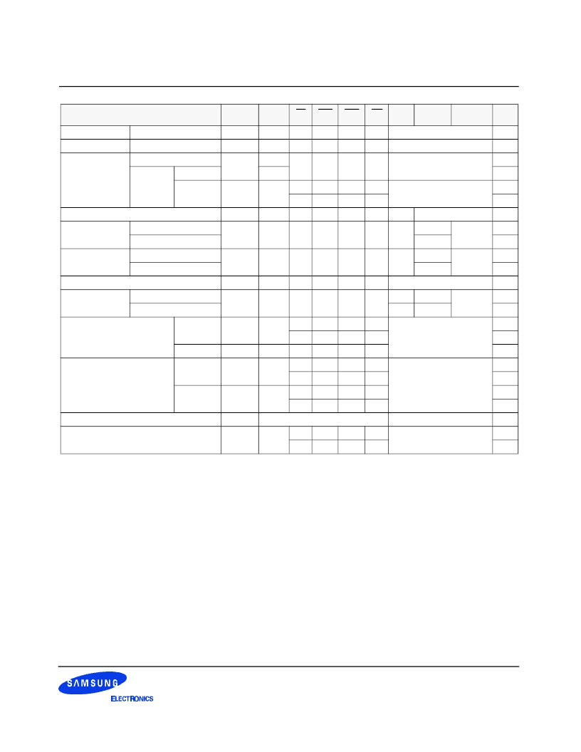
4. Command Truth Table
Preliminary
Table 8. Command truth table
(V=Valid, X=Don
′
t Care, H=Logic High, L=Logic Low)
COMMAND
CKEn-1
CKEn
CS
RAS
CAS
WE
BA
0,1
A
10
/AP
A
11,
A
9
~ A
0
Note
Register
Extended MRS
H
X
L
L
L
L
OP CODE
Register
Mode Register Set
H
X
L
L
L
L
OP CODE
1, 2
Refresh
Auto Refresh
H
H
L
L
L
H
X
3
Self
Refresh
Entry
L
3
Exit
L
H
L
H
H
H
X
3
H
X
X
X
3
Bank Active & Row Addr.
H
X
L
L
H
H
V
Row Address
Read &
Column Address
Auto Precharge Disable
H
X
L
H
L
H
V
L
Column
Address
4
Auto Precharge Enable
H
4
Write &
Column Address
Auto Precharge Disable
H
X
L
H
L
L
V
L
Column
Address
4
Auto Precharge Enable
H
4, 6
Burst Stop
H
X
L
H
H
L
X
7
Precharge
Bank Selection
H
X
L
L
H
L
V
L
X
All Banks
X
H
5
Active Power Down
Entry
H
L
H
X
X
X
X
L
V
V
V
Exit
L
H
X
X
X
X
Precharge Power Down Mode
Entry
H
L
H
X
X
X
X
L
H
H
H
Exit
L
H
H
X
X
X
L
V
V
V
DM
H
X
X
8
No operation (NOP) : Not defined
H
X
H
X
X
X
X
9
L
H
H
H
9
1. OP Code : Operand Code. A
0
~ A
11
& BA
0
~ BA
1
: Program keys. (@EMRS/MRS)
2.EMRS/ MRS can be issued only at all banks precharge state.
A new command can be issued 2 clock cycles after EMRS or MRS.
3. Auto refresh functions are same as the CBR refresh of DRAM.
The automatical precharge without row precharge command is meant by "Auto".
Auto/self refresh can be issued only at all banks precharge state.
4. BA
0
~ BA
1
: Bank select addresses.
If both BA
0
and BA
1
are "Low" at read, write, row active and precharge, bank A is selected.
If both BA
0
is "High" and BA
1
is "Low" at read, write, row active and precharge, bank B is selected.
If both BA
0
is "Low" and BA
1
is "High" at read, write, row active and precharge, bank C is selected.
If both BA
0
and BA
1
are "High" at read, write, row active and precharge, bank D is selected.
5. If A
10
/AP is "High" at row precharge, BA
0
and BA
1
are ignored and all banks are selected.
6. During burst write with auto precharge, new read/write command can not be issued.
Another bank read/write command can be issued after the end of burst.
New row active of the associated bank can be issued at t
RP
after the end of burst.
7. Burst stop command is valid at every burst length.
8. DM sampled at the rising and falling edges of the DQS and Data-in are masked at the both edges (Write DM latency is 0).
9. This combination is not defined for any function, which means "No Operation(NOP)" in DDR SDRAM.
相關(guān)PDF資料 |
PDF描述 |
|---|---|
| 25AV5-GA | FOR TV HORIZONTAL-DEFLECTION AMPLIFIER APPLICATIONS |
| 25CV100BE | Surface Mount Type Miniature, Super low profile 3.9mm height |
| 25CV10BE | Surface Mount Type Miniature, Super low profile 3.9mm height |
| 25CV68BE | Surface Mount Type Miniature, Super low profile 3.9mm height |
| 25CV22BE | Surface Mount Type Miniature, Super low profile 3.9mm height |
相關(guān)代理商/技術(shù)參數(shù) |
參數(shù)描述 |
|---|---|
| 256MB-FD | 制造商:PNY Technologies 功能描述:256MB USB, FOR IBM - Bulk |
| 256MB-FLASH | 制造商:STMicroelectronics 功能描述: |
| 256ME-250K | 制造商:ILLINOISCAPACITOR 制造商全稱:Illinois Capacitor, Inc. 功能描述:Metallized Polyester Motor Run/AC Film Capacitors In Boxes |
| 256ME-350K | 制造商:ILLINOISCAPACITOR 制造商全稱:Illinois Capacitor, Inc. 功能描述:Metallized Polyester Motor Run/AC Film Capacitors In Boxes |
| 256ME-400K | 制造商:ILLINOISCAPACITOR 制造商全稱:Illinois Capacitor, Inc. 功能描述:Metallized Polyester Motor Run/AC Film Capacitors In Boxes |
發(fā)布緊急采購,3分鐘左右您將得到回復(fù)。