- 您現(xiàn)在的位置:買賣IC網(wǎng) > PDF目錄36338 > 935262451518 (NXP SEMICONDUCTORS) COLOR SIGNAL DECODER, PQFP100 PDF資料下載
參數(shù)資料
| 型號: | 935262451518 |
| 廠商: | NXP SEMICONDUCTORS |
| 元件分類: | 顏色信號轉(zhuǎn)換 |
| 英文描述: | COLOR SIGNAL DECODER, PQFP100 |
| 封裝: | 14 X 14 X 1.40 MM, PLASTIC, SOT-407, LQFP-100 |
| 文件頁數(shù): | 32/144頁 |
| 文件大?。?/td> | 592K |
| 代理商: | 935262451518 |
第1頁第2頁第3頁第4頁第5頁第6頁第7頁第8頁第9頁第10頁第11頁第12頁第13頁第14頁第15頁第16頁第17頁第18頁第19頁第20頁第21頁第22頁第23頁第24頁第25頁第26頁第27頁第28頁第29頁第30頁第31頁當前第32頁第33頁第34頁第35頁第36頁第37頁第38頁第39頁第40頁第41頁第42頁第43頁第44頁第45頁第46頁第47頁第48頁第49頁第50頁第51頁第52頁第53頁第54頁第55頁第56頁第57頁第58頁第59頁第60頁第61頁第62頁第63頁第64頁第65頁第66頁第67頁第68頁第69頁第70頁第71頁第72頁第73頁第74頁第75頁第76頁第77頁第78頁第79頁第80頁第81頁第82頁第83頁第84頁第85頁第86頁第87頁第88頁第89頁第90頁第91頁第92頁第93頁第94頁第95頁第96頁第97頁第98頁第99頁第100頁第101頁第102頁第103頁第104頁第105頁第106頁第107頁第108頁第109頁第110頁第111頁第112頁第113頁第114頁第115頁第116頁第117頁第118頁第119頁第120頁第121頁第122頁第123頁第124頁第125頁第126頁第127頁第128頁第129頁第130頁第131頁第132頁第133頁第134頁第135頁第136頁第137頁第138頁第139頁第140頁第141頁第142頁第143頁第144頁
2000 Mar 15
127
Philips Semiconductors
Preliminary specication
PAL/NTSC/SECAM video decoder with adaptive PAL/NTSC
comb lter, VBI-data slicer and high performance scaler
SAA7114H
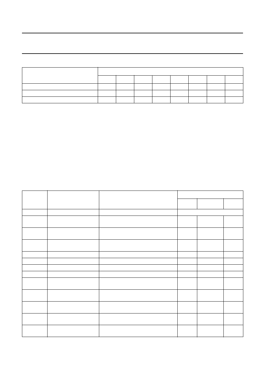
Table 126 Vertical luminance phase offset ‘00’; register set A (BCH[7:0]) and B (ECH[7:0])
16 PROGRAMMING START SET-UP
16.1
Decoder part
The given values force the following behaviour of the SAA7114H decoder part:
The analog input AI11 expects an NTSC M, PAL BDGHI or SECAM signal in CVBS format; analog anti-alias filter and
AGC active
Automatic field detection enabled
Standard ITU 656 output format enabled on expansion (X) port
Contrast, brightness and saturation control in accordance with ITU standards
Adaptive comb filter for luminance and chrominance activated
Pins LLC, LLC2, XTOUT, RTS0, RTS1 and RTCO are set to 3-state.
Table 127 Decoder part start set-up values for the three main standards
VERTICAL LUMINANCE PHASE
OFFSET
CONTROL BITS D7 TO D0
YPY07
YPY06
YPY05
YPY04
YPY03
YPY02
YPY01
YPY00
Offset = 0
0
000000
Offset = 32
32 = 1 line
0
100000
Offset = 255
32 lines
1
111111
SUB
ADDRESS
(HEX)
REGISTER
FUNCTION
BIT NAME(1)
VALUES (HEX)
NTSC M PAL BDGHI
SECAM
00
chip version
ID07 to ID04
read only
01
horizontal increment
delay
X, X, X, X, IDEL3 to IDEL0
08
02
analog input control 1
FUSE1 and FUSE0, GUDL1 to GUDL0,
MODE3 to MODE0
C0
03
analog input control 2
X, HLNRS, VBSL, WPOFF, HOLDG,
GAFIX, GAI28 and GAI18
10
04
analog input control 3
GAI17 to GAI10
90
05
analog input control 4
GAI27 to GAI20
90
06
horizontal sync start
HSB7 to HSB0
EB
07
horizontal sync stop
HSS7 to HSS0
E0
08
sync control
AUFD, FSEL, FOET, HTC1, HTC0,
HPLL, VNOI1 and VNOI0
98
09
luminance control
BYPS, YCOMB, LDEL, LUBW,
LUFI3 to LUFI0
40
1B
0A
luminance brightness
control
DBRI7 to DBRI0
80
0B
luminance contrast
control
DCON7 to DCON0
44
0C
chrominance saturation
control
DSAT7 to DSAT0
40
相關(guān)PDF資料 |
PDF描述 |
|---|---|
| 935262451557 | COLOR SIGNAL DECODER, PQFP100 |
| 935262469557 | SPECIALTY CONSUMER CIRCUIT, PQFP240 |
| 935263151557 | SPECIALTY CONSUMER CIRCUIT, PQFP240 |
| 935263331557 | SPECIALTY CONSUMER CIRCUIT, PQFP240 |
| 935263133112 | 26 W, 1 CHANNEL, AUDIO AMPLIFIER, PZIP17 |
相關(guān)代理商/技術(shù)參數(shù) |
參數(shù)描述 |
|---|---|
| 935264217557 | 制造商:NXP Semiconductors 功能描述:SUB ONLY IC |
| 935267356112 | 制造商:NXP Semiconductors 功能描述:IC TEA1507PN |
| 935268081112 | 制造商:NXP Semiconductors 功能描述:SUB ONLY IC |
| 935268721125 | 制造商:NXP Semiconductors 功能描述:Buffer/Line Driver 1-CH Non-Inverting 3-ST CMOS 5-Pin TSSOP T/R |
| 935269304128 | 制造商:ST-Ericsson 功能描述:IC AUDIO CODEC W/TCH SCRN 48LQFP |
發(fā)布緊急采購,3分鐘左右您將得到回復。