- 您現(xiàn)在的位置:買賣IC網(wǎng) > PDF目錄360656 > 9S12C128DGV1 MC9S12C Family Device User Guide PDF資料下載
參數(shù)資料
| 型號: | 9S12C128DGV1 |
| 英文描述: | MC9S12C Family Device User Guide |
| 中文描述: | MC9S12C家庭設(shè)備用戶指南 |
| 文件頁數(shù): | 64/136頁 |
| 文件大小: | 2190K |
| 代理商: | 9S12C128DGV1 |
第1頁第2頁第3頁第4頁第5頁第6頁第7頁第8頁第9頁第10頁第11頁第12頁第13頁第14頁第15頁第16頁第17頁第18頁第19頁第20頁第21頁第22頁第23頁第24頁第25頁第26頁第27頁第28頁第29頁第30頁第31頁第32頁第33頁第34頁第35頁第36頁第37頁第38頁第39頁第40頁第41頁第42頁第43頁第44頁第45頁第46頁第47頁第48頁第49頁第50頁第51頁第52頁第53頁第54頁第55頁第56頁第57頁第58頁第59頁第60頁第61頁第62頁第63頁當(dāng)前第64頁第65頁第66頁第67頁第68頁第69頁第70頁第71頁第72頁第73頁第74頁第75頁第76頁第77頁第78頁第79頁第80頁第81頁第82頁第83頁第84頁第85頁第86頁第87頁第88頁第89頁第90頁第91頁第92頁第93頁第94頁第95頁第96頁第97頁第98頁第99頁第100頁第101頁第102頁第103頁第104頁第105頁第106頁第107頁第108頁第109頁第110頁第111頁第112頁第113頁第114頁第115頁第116頁第117頁第118頁第119頁第120頁第121頁第122頁第123頁第124頁第125頁第126頁第127頁第128頁第129頁第130頁第131頁第132頁第133頁第134頁第135頁第136頁
Device User Guide — 9S12C128DGV1/D V01.10
64
2.4.4 VDDA, VSSA — Power Supply Pins for ATD and VREG
VDDA, VSSA are the power supply and ground input pins for the voltage regulator reference and the
analog to digital converter.
2.4.5 VRH, VRL — ATD Reference Voltage Input Pins
VRH and VRL are the reference voltage input pins for the analog to digital converter.
2.4.6 VDDPLL, VSSPLL — Power Supply Pins for PLL
Provides operating voltage and ground for the Oscillator and the Phased-Locked Loop. This allows the
supply voltage to the Oscillator and PLL to be bypassed independently. This 2.5V voltage is generated by
the internal voltage regulator.
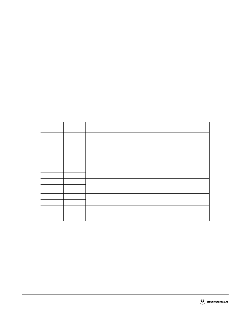
Table 2-2 MC9S12C-Family Power and Ground Connection Summary
Nominal
Voltage
VDD1
VDD2
allow an external source to supply the core VDD/VSS voltages and bypass
the internal voltage regulator.
In the 48 and 52 LQFP packages VDD2 and VSS2 are not available.
VSS2
VDDR
5.0 V
External power and ground, supply to internal voltage regulator.
VSSR
0 V
VDDX
5.0 V
External power and ground, supply to pin drivers.
VSSX
0 V
VDDA
5.0 V
Operating voltage and ground for the analog-to-digital converters and the
reference for the internal voltage regulator, allows the supply voltage to the
A/D to be bypassed independently.
VRH
5.0 V
Reference voltage low for the ATD converter.
In the 48 and 52 LQFP packages VRL is bonded to VSSA.
VRL
0 V
VDDPLL
2.5 V
Provides operating voltage and ground for the Phased-Locked Loop. This
allows the supply voltage to the PLL to be bypassed independently.
Internal power and ground generated by internal regulator.
NOTE:
All VSS pins must be connected together in the application. Because fast signal transitions
place high, short-duration current demands on the power supply, use bypass capacitors with
high-frequency characteristics and place them as close to the MCU as possible. Bypass requirements
depend on MCU pin load.
Section 3 System Clock Description
Mnemonic
Description
2.5 V
Internal power and ground generated by internal regulator. These also
VSS1
0V
VSSA
0 V
VSSPLL
0 V
F
For More Information On This Product,
Go to: www.freescale.com
n
.
相關(guān)PDF資料 |
PDF描述 |
|---|---|
| 9S12D32DGV1 | 9S12DGDJ64DGV1 Device Guide. also covers 9S12D64. 9S12A64. 9S12D32. and 9S12A32 devices |
| 9S12DJ64DGV1 | 9S12DJ64DG Device Guide. also covers 9S12D64. 9S12A64. 9S12D32 and 9S12A32 devices |
| 9S12DJ64-ZIP_PART2 | MC9S12DJ64 Users Guides. zip format. part 2 |
| 9S12DP256BDGV2 | 9S12Dx256B Device Guide. also covers C derivatives and 9S12Ax256 devices |
| 9S12DP512DGV1 | 9S12Dx512 Device Guide |
相關(guān)代理商/技術(shù)參數(shù) |
參數(shù)描述 |
|---|---|
| 9S12D32DGV1 | 制造商:未知廠家 制造商全稱:未知廠家 功能描述:9S12DGDJ64DGV1 Device Guide. also covers 9S12D64. 9S12A64. 9S12D32. and 9S12A32 devices |
| 9S12DJ64DGV1 | 制造商:未知廠家 制造商全稱:未知廠家 功能描述:9S12DJ64DG Device Guide. also covers 9S12D64. 9S12A64. 9S12D32 and 9S12A32 devices |
| 9S12DP256BDGV1 | 制造商:FREESCALE 制造商全稱:Freescale Semiconductor, Inc 功能描述:Automotive applications |
| 9S12DP256BDGV2 | 制造商:未知廠家 制造商全稱:未知廠家 功能描述:9S12Dx256B Device Guide. also covers C derivatives and 9S12Ax256 devices |
| 9S12DP512DGV1 | 制造商:未知廠家 制造商全稱:未知廠家 功能描述:9S12Dx512 Device Guide |
發(fā)布緊急采購,3分鐘左右您將得到回復(fù)。