- 您現(xiàn)在的位置:買賣IC網(wǎng) > PDF目錄373891 > AD6636BC (Analog Devices, Inc.) 150 MSPS Wideband Digital Down-Converter (DDC) PDF資料下載
參數(shù)資料
| 型號: | AD6636BC |
| 廠商: | Analog Devices, Inc. |
| 元件分類: | 數(shù)字上/下變頻 |
| 英文描述: | 150 MSPS Wideband Digital Down-Converter (DDC) |
| 中文描述: | 150MSPS的寬帶數(shù)字下變頻器(DDC) |
| 文件頁數(shù): | 43/72頁 |
| 文件大小: | 1629K |
| 代理商: | AD6636BC |
第1頁第2頁第3頁第4頁第5頁第6頁第7頁第8頁第9頁第10頁第11頁第12頁第13頁第14頁第15頁第16頁第17頁第18頁第19頁第20頁第21頁第22頁第23頁第24頁第25頁第26頁第27頁第28頁第29頁第30頁第31頁第32頁第33頁第34頁第35頁第36頁第37頁第38頁第39頁第40頁第41頁第42頁當前第43頁第44頁第45頁第46頁第47頁第48頁第49頁第50頁第51頁第52頁第53頁第54頁第55頁第56頁第57頁第58頁第59頁第60頁第61頁第62頁第63頁第64頁第65頁第66頁第67頁第68頁第69頁第70頁第71頁第72頁
AD6636
When the channel sync select bit of the AGC control register is
Logic 1, the AGC receives the SYNC signal used by the NCO of
the corresponding channel for the start. When this bit is Logic 0,
the pin sync defined by the 2-bit SYNC pin select word in the
AGC control register is used to provide the sync to the AGC.
Apart from these two methods, the AGC control register also
has a sync now bit that can be used to provide a sync to the
AGC by writing to this register through the microport or serial
port.
Rev. 0 | Page 43 of 72
PARALLEL PORT OUTPUT
The AD6636 incorporates three independent 16-bit parallel
ports for output data transfer. The three parallel output ports
share a common clock, PCLK. Each port consists of a 16-bit
data bus, REQuest signal, ACKnowledge signal, three channel
indicator pins, one I/Q indicator pin, one gain word indicator
pin, and a common shared PCLK pin. The parallel ports can be
configured to function in master mode or slave mode. By
default, the parallel ports are in slave mode on power-up.
Sync Process
Regardless of how a sync signal is received, the syncing process
is the same. When a sync is received, a start hold-off counter is
loaded with the 16-bit value in the AGC hold-off register, which
initiates the countdown. The countdown is based on the ADC
input clock. When the count reaches 1, a sync is initiated. When
a sync is initiated, the CIC decimation filter dumps the current
value to the square root, error estimation, and loop filter blocks.
After dumping the current value, it starts working toward the
next update value. Additionally on a sync, AGC can be
initialized if the initialize AGC on sync bit is set in the AGC
control register. During initialization, the CIC accumulator is
cleared and new values for CIC decimation, number of
averaging samples, CIC scale, signal gain, open-loop gains K
1
and K
2
, and pole parameter P are loaded from their respective
registers. When the initialize on sync bit is cleared, these
parameters are not loaded from the registers.
Each parallel port can output data from any or all of the AGCs,
using the 1-bit enable bit for each AGC in the parallel port
control register. Even when the AGC is not required for a
certain channel, the AGC can be bypassed, but the data is still
received from the bypassed AGC. The parallel port functionality
is programmable through the two parallel port control registers.
Each parallel port can be programmed individually to operate
in either interleaved I/Q mode or parallel I/Q mode. The mode
is selected using a 1-bit data format bit in the parallel port
control register. In both modes, the AGC gain word output can
be enabled using a 1-bit append gain bit in the parallel port
control register for individual output ports. There are six enable
bits per output port, one for each AGC in the corresponding
parallel port.
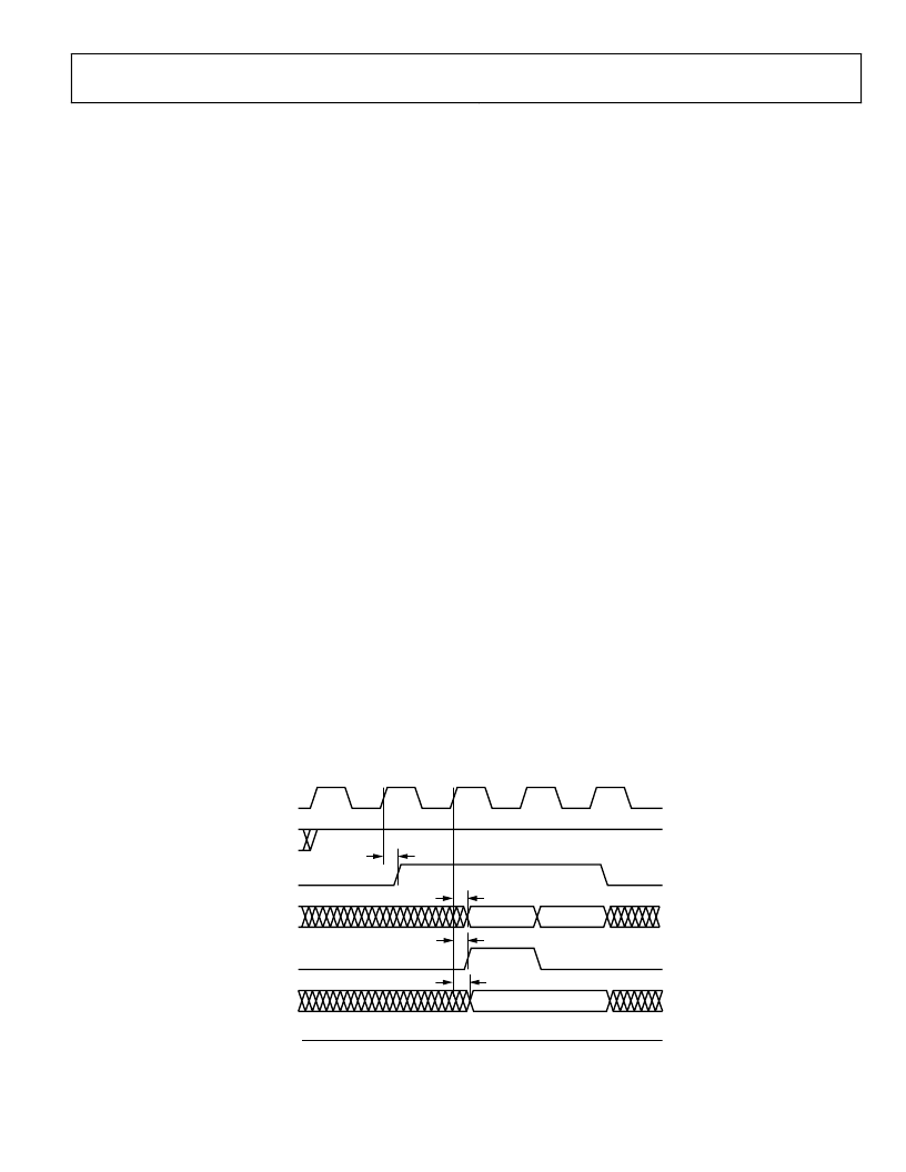
Interleaved I/Q Mode
Parallel port channel mode is selected by writing a 0 to the data
format bit for the parallel port in consideration. In this mode, I
and Q words from the AGC are output on the same 16-bit data
bus on a time-multiplexed basis. The 16-bit I word is output
followed by the 16-bit Q word. The specific AGCs output by the
port are selected by setting individual bits for each of the AGCs
in the parallel port control register. Figure 40 shows the timing
diagram for the interleaved I/Q mode.
This sync process is also initiated when a channel comes out of
sleep by using the start sync to the NCO. An additional feature
is the first sync only bit in the AGC control register. When this
bit is set, only the first sync initiates the process and the
remaining sync signals are ignored. This is useful when syncing
using a pin sync. A sync is required only on the first pulse on
this pin. These additional features make AGC synchronization
more flexible and applicable to varied circumstances.
PCLKn
t
DPREQ
PxREQ
PxACK
t
DPP
Px [15:0]
I [15:0]
Q [15:0]
PxIQ
t
DPIC
PxCH [2:0]
PxCH [2:0] = CHANNEL NO.
t
DPCH
PxGAIN
LOGIC LOW ‘0’
0
Figure 40. Interleaved I/Q Mode without an AGC Gain Word
相關PDF資料 |
PDF描述 |
|---|---|
| AD6636CBCZ1 | 150 MSPS Wideband Digital Down-Converter (DDC) |
| AD6636PCB | 150 MSPS Wideband Digital Down-Converter (DDC) |
| AD664(中文) | Monolithic 12-Bit Quad DAC(單片12位四D/A轉(zhuǎn)換器) |
| AD6640 | 12-Bit, 65 MSPS IF Sampling A/D Converter |
| AD6640AST | 12-Bit, 65 MSPS IF Sampling A/D Converter |
相關代理商/技術參數(shù) |
參數(shù)描述 |
|---|---|
| AD6636BC/PCB | 制造商:Analog Devices 功能描述:Evaluation Board For 150MSPS Wideband Digital Down-Converter 制造商:Analog Devices 功能描述:EVALUATION BOARD AD6636 - Bulk |
| AD6636BC/PCBZ | 制造商:Analog Devices 功能描述:Evaluation Kit For 150 MSPS, Wide Band, Digital Down Converter 制造商:Analog Devices 功能描述:EVALUATION BOARD AD6636 - Bulk |
| AD6636CBC | 制造商:Rochester Electronics LLC 功能描述: 制造商:Analog Devices 功能描述: |
| AD6636CBCZ | 功能描述:IC DIGITAL DWNCONV 4CH 256CSPBGA RoHS:是 類別:RF/IF 和 RFID >> RF 混頻器 系列:AD6636 產(chǎn)品培訓模塊:Lead (SnPb) Finish for COTS Obsolescence Mitigation Program 標準包裝:100 系列:- RF 型:W-CDMA 頻率:2.11GHz ~ 2.17GHz 混頻器數(shù)目:1 增益:17dB 噪音數(shù)據(jù):2.2dB 次要屬性:- 電流 - 電源:11.7mA 電源電壓:2.7 V ~ 3.3 V 包裝:托盤 封裝/外殼:12-VFQFN 裸露焊盤 供應商設備封裝:12-QFN-EP(3x3) |
| AD6636CBCZ1 | 制造商:AD 制造商全稱:Analog Devices 功能描述:150 MSPS Wideband Digital Down-Converter (DDC) |
發(fā)布緊急采購,3分鐘左右您將得到回復。