- 您現(xiàn)在的位置:買(mǎi)賣(mài)IC網(wǎng) > PDF目錄378286 > ADV7183AKST (ANALOG DEVICES INC) Multiformat SDTV Video Decoder PDF資料下載
參數(shù)資料
| 型號(hào): | ADV7183AKST |
| 廠商: | ANALOG DEVICES INC |
| 元件分類: | 顏色信號(hào)轉(zhuǎn)換 |
| 英文描述: | Multiformat SDTV Video Decoder |
| 中文描述: | COLOR SIGNAL DECODER, PQFP80 |
| 封裝: | LEAD FREE, MS-026-BEC, LQFP-80 |
| 文件頁(yè)數(shù): | 101/104頁(yè) |
| 文件大?。?/td> | 894K |
| 代理商: | ADV7183AKST |
第1頁(yè)第2頁(yè)第3頁(yè)第4頁(yè)第5頁(yè)第6頁(yè)第7頁(yè)第8頁(yè)第9頁(yè)第10頁(yè)第11頁(yè)第12頁(yè)第13頁(yè)第14頁(yè)第15頁(yè)第16頁(yè)第17頁(yè)第18頁(yè)第19頁(yè)第20頁(yè)第21頁(yè)第22頁(yè)第23頁(yè)第24頁(yè)第25頁(yè)第26頁(yè)第27頁(yè)第28頁(yè)第29頁(yè)第30頁(yè)第31頁(yè)第32頁(yè)第33頁(yè)第34頁(yè)第35頁(yè)第36頁(yè)第37頁(yè)第38頁(yè)第39頁(yè)第40頁(yè)第41頁(yè)第42頁(yè)第43頁(yè)第44頁(yè)第45頁(yè)第46頁(yè)第47頁(yè)第48頁(yè)第49頁(yè)第50頁(yè)第51頁(yè)第52頁(yè)第53頁(yè)第54頁(yè)第55頁(yè)第56頁(yè)第57頁(yè)第58頁(yè)第59頁(yè)第60頁(yè)第61頁(yè)第62頁(yè)第63頁(yè)第64頁(yè)第65頁(yè)第66頁(yè)第67頁(yè)第68頁(yè)第69頁(yè)第70頁(yè)第71頁(yè)第72頁(yè)第73頁(yè)第74頁(yè)第75頁(yè)第76頁(yè)第77頁(yè)第78頁(yè)第79頁(yè)第80頁(yè)第81頁(yè)第82頁(yè)第83頁(yè)第84頁(yè)第85頁(yè)第86頁(yè)第87頁(yè)第88頁(yè)第89頁(yè)第90頁(yè)第91頁(yè)第92頁(yè)第93頁(yè)第94頁(yè)第95頁(yè)第96頁(yè)第97頁(yè)第98頁(yè)第99頁(yè)第100頁(yè)當(dāng)前第101頁(yè)第102頁(yè)第103頁(yè)第104頁(yè)
ADV7183A
Digital Inputs
The digital inputs on the ADV7183A were designed to work
with 3.3 V signals, and are not tolerant of 5 V signals. Extra
components are needed if 5 V logic signals are required to be
applied to the decoder.
Antialiasing Filters
For inputs from some video sources that are not bandwidth
limited, signals outside the video band can alias back into the
video band during A/D conversion and appear as noise on the
output video. The ADV7183A oversamples the analog inputs by
a factor of 4. This 54 MHz sampling frequency reduces the
requirement for an input filter; for optimal performance it is
recommended that an antialiasing filter be employed. The
recommended low cost circuit for implementing this buffer and
filter circuit for all analog input signals is shown in Figure 41.
Rev. A | Page 101 of 104
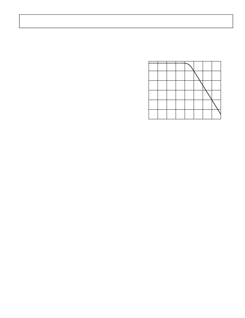
The buffer is a simple emitter-follower using a single npn
transistor. The antialiasing filter is implemented using passive
components. The passive filter is a third-order Butterworth
filter with a -3dB point of 9MHz. The frequency response of the
passive filter is shown in Figure 40. The flat pass band up to
6 MHz is essential. The attenuation of the signal at the output of
the filter due to the voltage divider of R24 and R63 is compen-
sated for in the ADV7183A part using the automatic gain
control. The ac coupling capacitor at the input to the buffer
creates a high-pass filter with the biasing resistors for the
transistor. This filter has a cut-off of
{2 × π × (R39||R89) × C93}
–1
= 0.62 Hz
It is essential that the cutoff of this filter be less than 1 Hz to
ensure correct operation of the internal clamps within the part.
These clamps ensure that the video stays within the 5 V range of
the op amp used.
0
–20
–40
–60
–80
–100
–120
100kHz
30MHz
10MHz
3MHz
1MHz
300kHz
300MHz
1GHz
100MHz
0
FREQUENCY
Figure 40. Third-Order Butterworth Filter Response
相關(guān)PDF資料 |
PDF描述 |
|---|---|
| ADV7330 | Multiformat 11-Bit Triple DAC Video Encoder |
| ADV7330KST | Multiformat 11-Bit Triple DAC Video Encoder |
| ADXL321 | Small and Thin 18 g Accelerometer |
| ADXL321EB | Small and Thin 18 g Accelerometer |
| ADXL321JCP | Small and Thin 18 g Accelerometer |
相關(guān)代理商/技術(shù)參數(shù) |
參數(shù)描述 |
|---|---|
| ADV7183AKST-U1 | 制造商:Analog Devices 功能描述:VID DECODER 80LQFP - Bulk |
| ADV7183AKST-X2 | 制造商:Analog Devices 功能描述:VID DECODER - Bulk |
| ADV7183AXST | 制造商:Analog Devices 功能描述:VIDEO DECODER I.C. - Bulk |
| ADV7183AXST-X2 | 制造商:Analog Devices 功能描述:VIDEO DECODER I.C. - Bulk |
| ADV7183AXT | 制造商:Analog Devices 功能描述:VIDEO DECODER I.C. - Bulk |
發(fā)布緊急采購(gòu),3分鐘左右您將得到回復(fù)。