- 您現(xiàn)在的位置:買賣IC網(wǎng) > PDF目錄298975 > CY3930V484-125BBC (Cypress Semiconductor Corp.) CPLDs at FPGA Densities PDF資料下載
參數(shù)資料
| 型號: | CY3930V484-125BBC |
| 廠商: | Cypress Semiconductor Corp. |
| 英文描述: | CPLDs at FPGA Densities |
| 中文描述: | CPLD器件在FPGA的密度 |
| 文件頁數(shù): | 2/86頁 |
| 文件大小: | 1212K |
| 代理商: | CY3930V484-125BBC |
第1頁當前第2頁第3頁第4頁第5頁第6頁第7頁第8頁第9頁第10頁第11頁第12頁第13頁第14頁第15頁第16頁第17頁第18頁第19頁第20頁第21頁第22頁第23頁第24頁第25頁第26頁第27頁第28頁第29頁第30頁第31頁第32頁第33頁第34頁第35頁第36頁第37頁第38頁第39頁第40頁第41頁第42頁第43頁第44頁第45頁第46頁第47頁第48頁第49頁第50頁第51頁第52頁第53頁第54頁第55頁第56頁第57頁第58頁第59頁第60頁第61頁第62頁第63頁第64頁第65頁第66頁第67頁第68頁第69頁第70頁第71頁第72頁第73頁第74頁第75頁第76頁第77頁第78頁第79頁第80頁第81頁第82頁第83頁第84頁第85頁第86頁
Delta39K ISR
CPLD Family
Document #: 38-03039 Rev. *H
Page 10 of 86
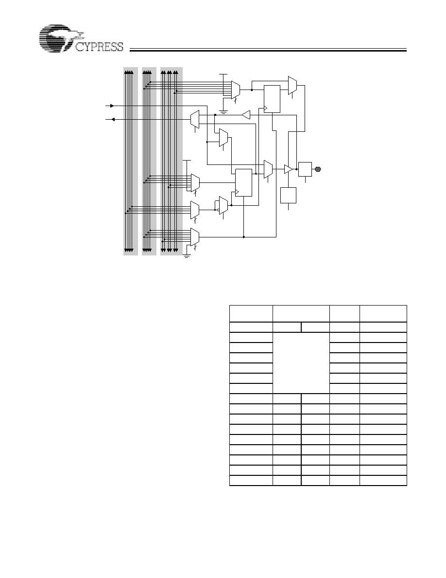
I/O Signals
There are four dedicated inputs (GCTL[3:0]) that are used as
Global I/O Control Signals available to every I/O cell. These
global I/O control signals may be used as output enables,
register resets and register clock enables as shown in
Figure 8. These global control signals, driven from four
dedicated pins, can only be used as active-high signals and
are available only to the I/O cells thereby implementing fast
resets, register and output enables.
In addition, there are six OCC signals available to each I/O
cell. These control signals may be used as output enables,
register resets and register clock enables as shown in
Figure 8. Unlike global control signals, these OCC signal can
be driven from internal logic or and I/O pin.
One of the four global clocks can be selected as the clock for
the I/O cell register. The clock mux output is an input to a clock
polarity mux that allows the input/output register to be clocked
on either edge of the clock
Slew Rate Control
The output buffer has a slew rate control option. This allows
the output buffer to slew at a fast rate (3 V/ns) or a slow rate
(1 V/ns). All I/Os default to fast slew rate. For designs
concerned with meeting FCC emissions standards the slow
edge provides for lower system noise. For designs requiring
very high performance the fast edge rate provides maximum
system performance.
DQ
RES
E
G
lobal
I/O
C
ontr
o
lSi
gnal
s
O
u
tput
C
ontr
o
lC
hannel
O
C
G
lobal
C
loc
k
Si
gnal
s
Slew
Rate
Control
C
I/O
From
Output PIM
To Routing
Channel
OE Mux
Register Input
Mux
Register Enable
Mux
Output Mux
Clock Mux
Clock
Polarity
Mux
Register Reset
Mux
Input
Mux
Bus
Hold
C
DQ
RES
C
Registered OE
Mux
C
3
C
3
C
2
3
C
Figure 8. Block Diagram of I/O Cell
Table 3.
I/O Standards
I/O
Standard
VREF (V)
VCCIO
Termination
Voltage (VTT)
Min.
Max.
LVTTL
N/A
3.3V
N/A
LVCMOS
3.3V
N/A
LVCMOS3
3.0V
N/A
LVCMOS2
2.5V
N/A
LVCMOS18
1.8V
N/A
3.3V PCI
3.3V
N/A
GTL+
0.9
1.1
N/A
1.5
SSTL3 I
1.3
1.7
3.3V
1.5
SSTL3 II
1.3
1.7
3.3V
1.5
SSTL2 I
1.15
1.35
2.5V
1.25
SSTL2 II
1.15
1.35
2.5V
1.25
HSTL I
0.68
0.9
1.5V
0.75
HSTL II
0.68
0.9
1.5V
0.75
HSTL III
0.68
0.9
1.5V
1.5
HSTL IV
0.68
0.9
1.5V
1.5
相關PDF資料 |
PDF描述 |
|---|---|
| CY3950V484-125BBC | CPLDs at FPGA Densities |
| CY54FCT540CTDMB | FCT SERIES, 8-BIT DRIVER, INVERTED OUTPUT, CDIP20 |
| CY54FCT543CTDMB | FCT SERIES, 8-BIT REGISTERED TRANSCEIVER, TRUE OUTPUT, CDIP24 |
| CY54FCT543ATDMB | FCT SERIES, 8-BIT REGISTERED TRANSCEIVER, TRUE OUTPUT, CDIP24 |
| CY54FCT543ATLMB | FCT SERIES, 8-BIT REGISTERED TRANSCEIVER, TRUE OUTPUT, CQCC28 |
相關代理商/技術參數(shù) |
參數(shù)描述 |
|---|---|
| CY3930V484-125BBI | 制造商:CYPRESS 制造商全稱:Cypress Semiconductor 功能描述:CPLDs at FPGA Densities |
| CY3930V484-125BGC | 制造商:CYPRESS 制造商全稱:Cypress Semiconductor 功能描述:CPLDs at FPGA Densities |
| CY3930V484-125BGI | 制造商:CYPRESS 制造商全稱:Cypress Semiconductor 功能描述:CPLDs at FPGA Densities |
| CY3930V484-125MBC | 制造商:CYPRESS 制造商全稱:Cypress Semiconductor 功能描述:CPLDs at FPGA Densities |
| CY3930V484-125MBI | 制造商:CYPRESS 制造商全稱:Cypress Semiconductor 功能描述:CPLDs at FPGA Densities |
發(fā)布緊急采購,3分鐘左右您將得到回復。