- 您現(xiàn)在的位置:買賣IC網(wǎng) > PDF目錄298975 > CY7C1339B-133BGIT (CYPRESS SEMICONDUCTOR CORP) 128K X 32 CACHE SRAM, 4 ns, PBGA119 PDF資料下載
參數(shù)資料
| 型號(hào): | CY7C1339B-133BGIT |
| 廠商: | CYPRESS SEMICONDUCTOR CORP |
| 元件分類: | SRAM |
| 英文描述: | 128K X 32 CACHE SRAM, 4 ns, PBGA119 |
| 封裝: | 14 X 22 MM, 2.40 MM HEIGHT, PLASTIC, BGA-119 |
| 文件頁數(shù): | 12/17頁 |
| 文件大小: | 527K |
| 代理商: | CY7C1339B-133BGIT |
CY7C1339B
Document #: 38-05141 Rev. *A
Page 4 of 17
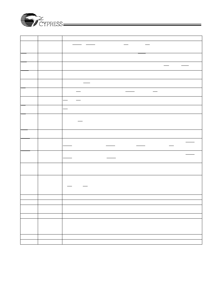
Pin Definitions
Pin Name
I/O
Pin Description
A[16:0]
Input-
Synchronous
Address Inputs used to select one of the 64K address locations. Sampled at the rising edge of the
CLK if ADSP or ADSC is active LOW, and CE1, CE2, and CE3 are sampled active. A[1:0] feed the
two-bit counter.
BW[3:0]
Input-
Synchronous
Byte Write Select Inputs, active LOW. Qualified with BWE to conduct byte writes to the SRAM.
Sampled on the rising edge of CLK.
GW
Input-
Synchronous
Global Write Enable Input, active LOW. When asserted LOW on the rising edge of CLK, a global
Write is conducted (ALL bytes are written, regardless of the values on BW[3:0] and BWE).
BWE
Input-
Synchronous
Byte Write Enable Input, active LOW. Sampled on the rising edge of CLK. This signal must be
asserted LOW to conduct a Byte Write.
CLK
Input-Clock
Clock Input. Used to capture all synchronous inputs to the device. Also used to increment the burst
counter when ADV is asserted LOW, during a burst operation.
CE1
Input-
Synchronous
Chip Enable 1 Input, active LOW. Sampled on the rising edge of CLK. Used in conjunction with
CE2 and CE3 to select/deselect the device. ADSP is ignored if CE1 is HIGH.
CE2
Input-
Synchronous
Chip Enable 2 Input, active HIGH. Sampled on the rising edge of CLK. Used in conjunction with
CE1 and CE3 to select/deselect the device.
CE3
Input-
Synchronous
Chip Enable 3 Input, active LOW. Sampled on the rising edge of CLK. Used in conjunction with
CE1 and CE2 to select/deselect the device.
OE
Input-
Asynchronous
Output Enable, Asynchronous Input, active LOW. Controls the direction of the I/O pins. When LOW,
the I/O pins behave as outputs. When deserted HIGH, I/O pins are three-stated, and act as input
data pins. OE is masked during the first clock of a Read cycle when emerging from a deselected
state.
ADV
Input-
Synchronous
Advance Input Signal, sampled on the rising edge of CLK. When asserted, it automatically incre-
ments the address in a burst cycle.
ADSP
Input-
Synchronous
Address Strobe from Processor, sampled on the rising edge of CLK. When asserted LOW, A[16:0]
is captured in the address registers. A[1:0] are also loaded into the burst counter. When ADSP and
ADSC are both asserted, only ADSP is recognized. ASDP is ignored when CE1 is deserted HIGH.
ADSC
Input-
Synchronous
Address Strobe from Controller, sampled on the rising edge of CLK. When asserted LOW, A[16:0]
is captured in the address registers. A[1:0] are also loaded into the burst counter. When ADSP and
ADSC are both asserted, only ADSP is recognized.
ZZ
Input-
Asynchronous
ZZ “sleep” Input. This active HIGH input places the device in a non-time-critical “sleep” condition
with data integrity preserved. Leaving ZZ floating or NC will default the device into an active state.
ZZ has an internal pull down.
DQ[31:0]
I/O-
Synchronous
Bidirectional Data I/O Lines. As inputs, they feed into an on-chip data register that is triggered by
the rising edge of CLK. As outputs, they deliver the data contained in the memory location specified
by A[16:0] during the previous clock rise of the Read cycle. The direction of the pins is controlled
by OE. When OE is asserted LOW, the pins behave as outputs. When HIGH, DQ[31:0] are placed
in a three-state condition.
VDD
Power Supply Power supply inputs to the core of the device. Should be connected to 3.3V power supply.
VSS
Ground
Ground for the core of the device. Should be connected to ground of the system.
VDDQ
I/O Power
Supply
Power supply for the I/O circuitry. Should be connected to a 3.3V or 2.5V power supply.
VSSQ
I/O Ground
Ground for the I/O circuitry. Should be connected to ground of the system.
MODE
Input-
Static
Selects Burst Order. When tied to GND selects linear burst sequence. When tied to VDDQ or left
floating selects interleaved burst sequence. This is a strap pin and should remain static during
device operation. When left floating or NC, defaults to interleaved burst order. Mode pin has an
internal pull up.
NC
–
No Connects.
DNU
-
Do Not Use pins. These pins could be left floating or tied to GND.
相關(guān)PDF資料 |
PDF描述 |
|---|---|
| CY7C1339G-200AXCT | 128K X 32 CACHE SRAM, 2.8 ns, PQFP100 |
| CY7C1347D-250BGC | 128K X 36 CACHE SRAM, 2.4 ns, PBGA119 |
| CY7C1512JV18-267BZXC | 4M X 18 QDR SRAM, 0.45 ns, PBGA165 |
| CY7C1515AV18-250BZXI | 2M X 36 QDR SRAM, 0.45 ns, PBGA165 |
| CY7C1522JV18-250BZI | 8M X 8 DDR SRAM, 0.45 ns, PBGA165 |
相關(guān)代理商/技術(shù)參數(shù) |
參數(shù)描述 |
|---|---|
| CY7C1339F-100AC | 制造商:Cypress Semiconductor 功能描述:SRAM Chip Sync Single 3.3V 4M-Bit 128K x 32 4.5ns 100-Pin TQFP |
| CY7C1339F-100BGI | 制造商:Cypress Semiconductor 功能描述: |
| CY7C1339F-100BGIT | 制造商:Cypress Semiconductor 功能描述:SRAM Chip Sync Single 3.3V 4M-Bit 128K x 32 4.5ns 119-Pin BGA T/R |
| CY7C1339F-133AC | 制造商:Cypress Semiconductor 功能描述:SRAM Chip Sync Single 3.3V 4M-Bit 128K x 32 4ns 100-Pin TQFP |
| CY7C1339F-166AC | 制造商:Rochester Electronics LLC 功能描述:128KX32 3.3V SYNC-PL SRAM (2.5/3.3V I/O) 1CD - Bulk |
發(fā)布緊急采購,3分鐘左右您將得到回復(fù)。