- 您現在的位置:買賣IC網 > PDF目錄170347 > CY8C5386AXI-081 (CYPRESS SEMICONDUCTOR CORP) MULTIFUNCTION PERIPHERAL, PQFP100 PDF資料下載
參數資料
| 型號: | CY8C5386AXI-081 |
| 廠商: | CYPRESS SEMICONDUCTOR CORP |
| 元件分類: | 外設及接口 |
| 英文描述: | MULTIFUNCTION PERIPHERAL, PQFP100 |
| 封裝: | 14 X 14 MM, 1.40 MM HEIGHT, ROHS COMPLAINT, MS-026, TQFP-100 |
| 文件頁數: | 16/102頁 |
| 文件大?。?/td> | 2374K |
| 代理商: | CY8C5386AXI-081 |
第1頁第2頁第3頁第4頁第5頁第6頁第7頁第8頁第9頁第10頁第11頁第12頁第13頁第14頁第15頁當前第16頁第17頁第18頁第19頁第20頁第21頁第22頁第23頁第24頁第25頁第26頁第27頁第28頁第29頁第30頁第31頁第32頁第33頁第34頁第35頁第36頁第37頁第38頁第39頁第40頁第41頁第42頁第43頁第44頁第45頁第46頁第47頁第48頁第49頁第50頁第51頁第52頁第53頁第54頁第55頁第56頁第57頁第58頁第59頁第60頁第61頁第62頁第63頁第64頁第65頁第66頁第67頁第68頁第69頁第70頁第71頁第72頁第73頁第74頁第75頁第76頁第77頁第78頁第79頁第80頁第81頁第82頁第83頁第84頁第85頁第86頁第87頁第88頁第89頁第90頁第91頁第92頁第93頁第94頁第95頁第96頁第97頁第98頁第99頁第100頁第101頁第102頁
PRELIMINARY
PSoC 5: CY8C53 Family Datasheet
Document Number: 001-55035 Rev. *G
Page 20 of 102
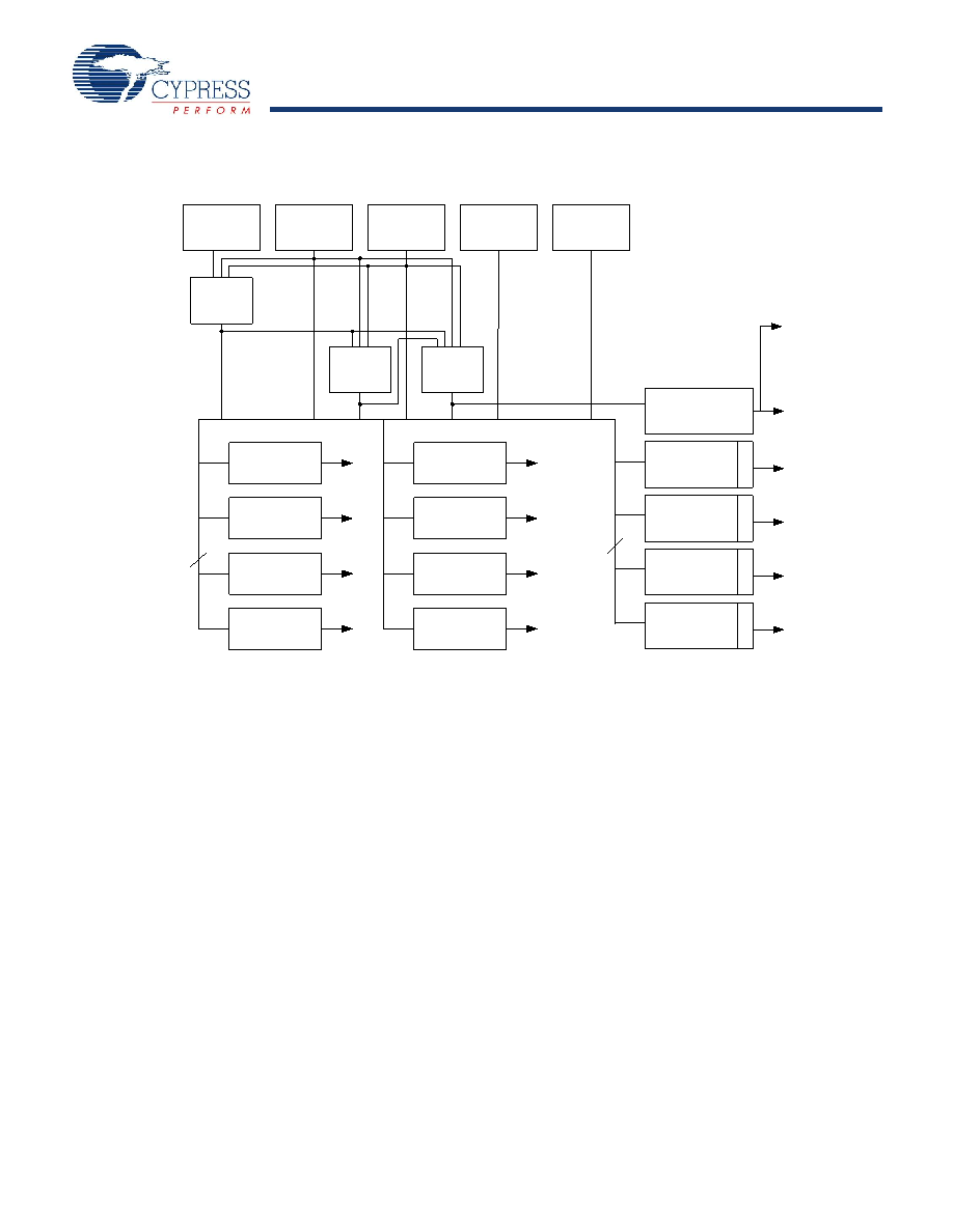
Figure 6-1. Clocking Subsystem
6.1.1 Internal Oscillators
6.1.1.1 Internal Main Oscillator
In most designs the IMO is the only clock source required, due
to its ±1% accuracy. The IMO operates with no external
components and outputs a stable clock. A factory trim for each
frequency range is stored in the device. With the factory trim,
tolerance varies from ±1% at 3 MHz, up to ±7% at 74 MHz. The
IMO, in conjunction with the PLL, allows generation of CPU and
system clocks up to the device's maximum frequency (see
The IMO provides clock outputs at 3-, 6-, 12-, 24-, 48-, and
74-MHz.
6.1.1.2 Clock Doubler
The clock doubler outputs a clock at twice the frequency of the
input clock. The doubler works for input frequency ranges of 6 to
24 MHz (providing 12 to 48 MHz at the output). It can be
configured to use a clock from the IMO, MHzECO, or the DSI
(external pin). The doubler is typically used to clock the USB.
6.1.1.3 Phase-Locked Loop
The PLL allows low frequency, high accuracy clocks to be
multiplied to higher frequencies. This is a tradeoff between
higher clock frequency and accuracy and, higher power
consumption and increased startup time.
The PLL block provides a mechanism for generating clock
frequencies based upon a variety of input sources. The PLL
outputs clock frequencies in the range of 24 to 80 MHz. Its input
and feedback dividers supply 4032 discrete ratios to create
almost any desired system clock frequency. The accuracy of the
PLL output depends on the accuracy of the PLL input source.
The most common PLL use is to multiply the IMO clock at 3 MHz,
where it is most accurate, to generate the CPU and system
clocks up to the device’s maximum frequency.
The PLL achieves phase lock within 250 s (verified by bit
setting). It can be configured to use a clock from the IMO,
MHzECO, or DSI (external pin). The PLL clock source can be
used until lock is complete and signaled with a lock bit. The lock
signal can be routed through the DSI to generate an interrupt.
Disable the PLL before entering low power modes.
6.1.1.4 Internal Low Speed Oscillator
The ILO provides clock frequencies for low power consumption,
including the watchdog timer, and sleep timer. The ILO
generates up to three different clocks: 1 kHz, 33 kHz, and
100 kHz.
The 1-kHz clock (CLK1K) is typically used for a background
‘heartbeat’ timer. This clock inherently lends itself to low power
supervisory operations such as the watchdog timer and long
sleep intervals using the central timewheel (CTW).
4-33 MHz
ECO
3-74 MHz
IMO
32 kHz ECO
1,33,100 kHz
ILO
s
k
e
w
7
Digital Clock
Divider 16 bit
Digital Clock
Divider 16 bit
Digital Clock
Divider 16 bit
Digital Clock
Divider 16 bit
Digital Clock
Divider 16 bit
Digital Clock
Divider 16 bit
Digital Clock
Divider 16 bit
Digital Clock
Divider 16 bit
Analog Clock
Divider 16 bit
Bus Clock Divider
16 bit
12-48 MHz
Doubler
24-80 MHz
PLL
System
Clock Mux
External IO
or DSI
0-66 MHz
s
k
e
w
Analog Clock
Divider 16 bit
s
k
e
w
Analog Clock
Divider 16 bit
s
k
e
w
Analog Clock
Divider 16 bit
Bus
Clock
CPU
Clock
相關PDF資料 |
PDF描述 |
|---|---|
| CYD18S72AV-133BBI | 256K X 72 DUAL-PORT SRAM, 5.5 ns, PBGA484 |
| CYDD18S72V18-167BGI | 256K X 72 DUAL-PORT SRAM, 9 ns, PBGA484 |
| CYW2330ZITR | PLL FREQUENCY SYNTHESIZER, 2500 MHz, PDSO20 |
| CYW311OXCT | 200 MHz, PROC SPECIFIC CLOCK GENERATOR, PDSO48 |
| CZ23EH-FREQ-OUT23 | VCXO, CLOCK, 1.25 MHz - 65 MHz, CMOS/TTL OUTPUT |
相關代理商/技術參數 |
參數描述 |
|---|---|
| CY8C5466AXI-064 | 功能描述:可編程片上系統 - PSoC PSoC 5 RoHS:否 制造商:Cypress Semiconductor 核心:8051 處理器系列:CY8C36 數據總線寬度:8 bit 最大時鐘頻率:67 MHz 程序存儲器大小:32 KB 數據 RAM 大小:4 KB 片上 ADC:Yes 工作電源電壓:0.5 V to 5.5 V 工作溫度范圍:- 40 C to + 85 C 封裝 / 箱體:QFN-68 安裝風格:SMD/SMT |
| CY8C5466AXI-064T | 功能描述:可編程片上系統 - PSoC 64Kb Flash 16Kb SRAM PSoC 5 RoHS:否 制造商:Cypress Semiconductor 核心:8051 處理器系列:CY8C36 數據總線寬度:8 bit 最大時鐘頻率:67 MHz 程序存儲器大小:32 KB 數據 RAM 大小:4 KB 片上 ADC:Yes 工作電源電壓:0.5 V to 5.5 V 工作溫度范圍:- 40 C to + 85 C 封裝 / 箱體:QFN-68 安裝風格:SMD/SMT |
| CY8C5466LTI-063 | 功能描述:可編程片上系統 - PSoC PSoC 5 RoHS:否 制造商:Cypress Semiconductor 核心:8051 處理器系列:CY8C36 數據總線寬度:8 bit 最大時鐘頻率:67 MHz 程序存儲器大小:32 KB 數據 RAM 大小:4 KB 片上 ADC:Yes 工作電源電壓:0.5 V to 5.5 V 工作溫度范圍:- 40 C to + 85 C 封裝 / 箱體:QFN-68 安裝風格:SMD/SMT |
| CY8C5466LTI-063T | 功能描述:可編程片上系統 - PSoC 64Kb Flash 16Kb SRAM PSoC 5 RoHS:否 制造商:Cypress Semiconductor 核心:8051 處理器系列:CY8C36 數據總線寬度:8 bit 最大時鐘頻率:67 MHz 程序存儲器大小:32 KB 數據 RAM 大小:4 KB 片上 ADC:Yes 工作電源電壓:0.5 V to 5.5 V 工作溫度范圍:- 40 C to + 85 C 封裝 / 箱體:QFN-68 安裝風格:SMD/SMT |
| CY8C5467AXI-011 | 功能描述:可編程片上系統 - PSoC PSoC 5 RoHS:否 制造商:Cypress Semiconductor 核心:8051 處理器系列:CY8C36 數據總線寬度:8 bit 最大時鐘頻率:67 MHz 程序存儲器大小:32 KB 數據 RAM 大小:4 KB 片上 ADC:Yes 工作電源電壓:0.5 V to 5.5 V 工作溫度范圍:- 40 C to + 85 C 封裝 / 箱體:QFN-68 安裝風格:SMD/SMT |
發(fā)布緊急采購,3分鐘左右您將得到回復。