- 您現(xiàn)在的位置:買賣IC網(wǎng) > PDF目錄170347 > CY8C5386AXI-081 (CYPRESS SEMICONDUCTOR CORP) MULTIFUNCTION PERIPHERAL, PQFP100 PDF資料下載
參數(shù)資料
| 型號: | CY8C5386AXI-081 |
| 廠商: | CYPRESS SEMICONDUCTOR CORP |
| 元件分類: | 外設及接口 |
| 英文描述: | MULTIFUNCTION PERIPHERAL, PQFP100 |
| 封裝: | 14 X 14 MM, 1.40 MM HEIGHT, ROHS COMPLAINT, MS-026, TQFP-100 |
| 文件頁數(shù): | 22/102頁 |
| 文件大?。?/td> | 2374K |
| 代理商: | CY8C5386AXI-081 |
第1頁第2頁第3頁第4頁第5頁第6頁第7頁第8頁第9頁第10頁第11頁第12頁第13頁第14頁第15頁第16頁第17頁第18頁第19頁第20頁第21頁當前第22頁第23頁第24頁第25頁第26頁第27頁第28頁第29頁第30頁第31頁第32頁第33頁第34頁第35頁第36頁第37頁第38頁第39頁第40頁第41頁第42頁第43頁第44頁第45頁第46頁第47頁第48頁第49頁第50頁第51頁第52頁第53頁第54頁第55頁第56頁第57頁第58頁第59頁第60頁第61頁第62頁第63頁第64頁第65頁第66頁第67頁第68頁第69頁第70頁第71頁第72頁第73頁第74頁第75頁第76頁第77頁第78頁第79頁第80頁第81頁第82頁第83頁第84頁第85頁第86頁第87頁第88頁第89頁第90頁第91頁第92頁第93頁第94頁第95頁第96頁第97頁第98頁第99頁第100頁第101頁第102頁
PRELIMINARY
PSoC 5: CY8C53 Family Datasheet
Document Number: 001-55035 Rev. *G
Page 26 of 102
The boost converter can be operated in two different modes:
active and standby. Active mode is the normal mode of operation
where the boost regulator actively generates a regulated output
voltage. In standby mode, most boost functions are disabled,
thus reducing power consumption of the boost circuit. The
converter can be configured to provide low power, low current
regulation in the standby mode. The external 32 kHz crystal can
be used to generate inductor boost pulses on the rising and
falling edge of the clock when the output voltage is less than the
programmed value. This is called automatic thump mode (ATM).
The boost typically draws 200 A in active mode and 12 A in
standby mode. The boost operating modes must be used in
conjunction with chip power modes to minimize the total chip
power consumption. Table 6-4 lists the boost power modes
available in different chip power modes.
The switching frequency can be set to 100 kHz, 400 kHz, 2 MHz,
or 32 kHz to optimize efficiency and component cost. The
100 kHz, 400 kHz, and 2 MHz switching frequencies are
generated using oscillators internal to the boost converter block.
When the 32 kHz switching frequency is selected, the clock is
derived from a 32 kHz external crystal oscillator. The 32 kHz
external clock is primarily intended for boost standby mode.
If the boost converter is not used in a given application, tie the
VBAT, VSSB, and VBOOST pins to ground and leave the Ind pin
unconnected.
6.3 Reset
CY8C53 has multiple internal and external reset sources
available. The reset sources are:
Power source monitoring - The analog and digital power
voltages, VDDA, VDDD, VCCA, and VCCD are monitored in
several different modes during power up, active mode, and
sleep mode (buzzing). If any of the voltages goes outside
predetermined ranges then a reset is generated. The monitors
are programmable to generate an interrupt to the processor
under certain conditions before reaching the reset thresholds.
External - The device can be reset from an external source by
pulling the reset pin (XRES) low. The XRES pin includes an
internal pull-up to Vddio1. VDDD, VDDA, and Vddio1 must all
have voltage applied before the part comes out of reset.
Watchdog timer - A watchdog timer monitors the execution of
instructions by the processor. If the watchdog timer is not reset
by firmware within a certain period of time, the watchdog timer
generates a reset.
Software - The device can be reset under program control.
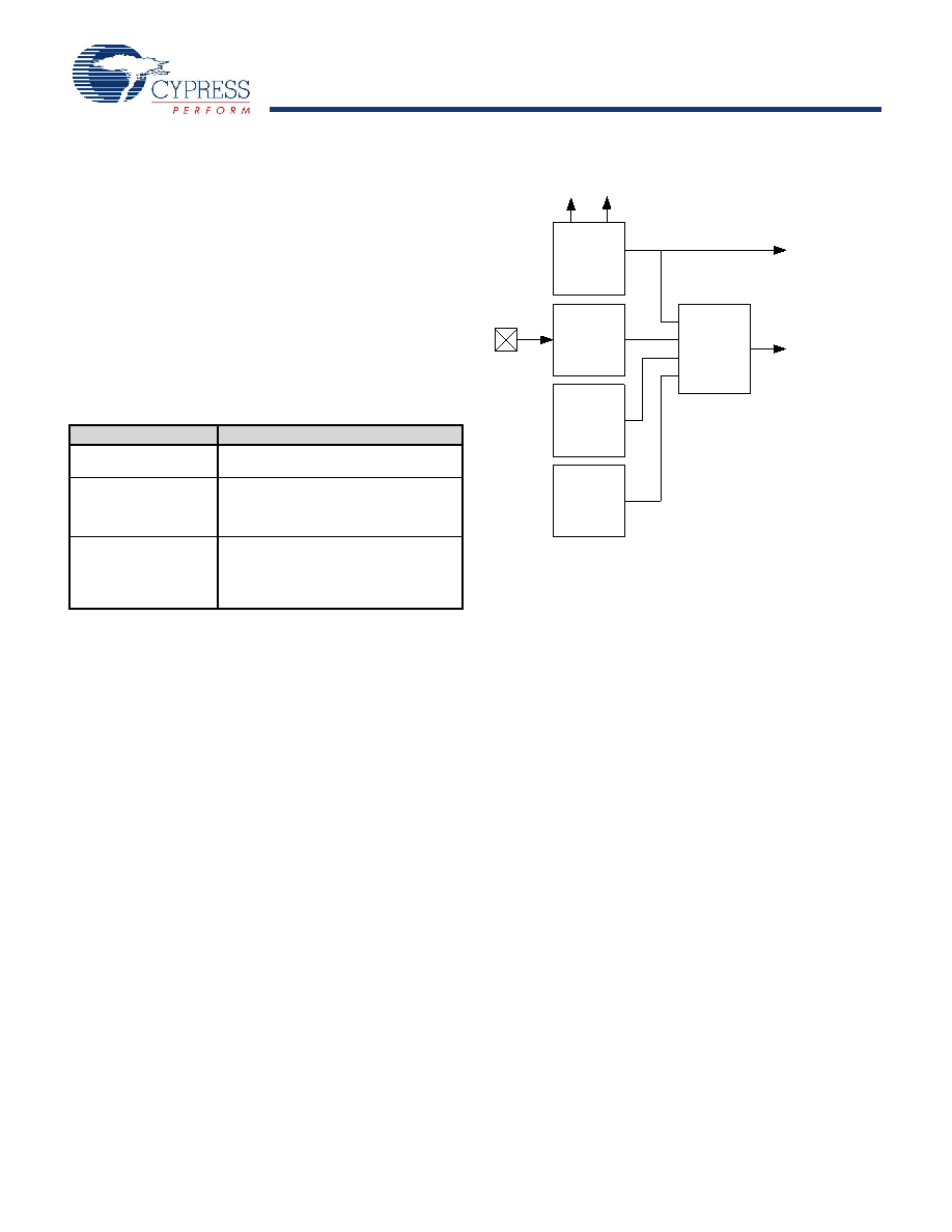
Figure 6-7. Resets
The term system reset indicates that the processor as well as
analog and digital peripherals and registers are reset.
A reset status register holds the source of the most recent reset
or power voltage monitoring interrupt. The program may
examine this register to detect and report exception conditions.
This register is cleared after a power on reset.
6.3.1 Reset Sources
6.3.1.1 Power Voltage Level Monitors
IPOR - Initial Power on Reset
At initial power on, IPOR monitors the power voltages VDDD
and VDDA, both directly at the pins and at the outputs of the
corresponding internal regulators. The trip level is not precise.
It is set to approximately 1 volt, which is below the lowest
specified operating voltage but high enough for the internal
circuits to be reset and to hold their reset state. The monitor
generates a reset pulse that is at least 100 ns wide. It may be
much wider if one or more of the voltages ramps up slowly.
To save power the IPOR circuit is disabled when the internal
digital supply is stable. Voltage supervision is then handed off
to the precise low voltage reset (PRES) circuit. When the
voltage is high enough for PRES to release, the IMO starts.
PRES - Precise Low Voltage Reset
This circuit monitors the outputs of the analog and digital
internal regulators after power up. The regulator outputs are
compared to a precise reference voltage. The response to a
PRES trip is identical to an IPOR reset.
Table 6-4. Chip and Boost Power Modes Compatibility
Chip Power Modes
Boost Power Modes
Chip -Active mode
Boost can be operated in either active or
standby mode.
Chip -Sleep mode
Boost can be operated in either active or
standby mode. However, it is recom-
mended to operate boost in standby
mode for low power consumption
Chip-Hibernate mode
Boost can only be operated in active
mode. However, it is recommended not to
use boost in chip hibernate mode due to
high current consumption in boost active
mode
Reset
Controller
Watchdog
Timer
External
Reset
Power
Voltage
Level
Monitors
Software
Reset
Register
Vddd Vdda
Reset
Pin
System
Reset
Processor
Interrupt
相關PDF資料 |
PDF描述 |
|---|---|
| CYD18S72AV-133BBI | 256K X 72 DUAL-PORT SRAM, 5.5 ns, PBGA484 |
| CYDD18S72V18-167BGI | 256K X 72 DUAL-PORT SRAM, 9 ns, PBGA484 |
| CYW2330ZITR | PLL FREQUENCY SYNTHESIZER, 2500 MHz, PDSO20 |
| CYW311OXCT | 200 MHz, PROC SPECIFIC CLOCK GENERATOR, PDSO48 |
| CZ23EH-FREQ-OUT23 | VCXO, CLOCK, 1.25 MHz - 65 MHz, CMOS/TTL OUTPUT |
相關代理商/技術參數(shù) |
參數(shù)描述 |
|---|---|
| CY8C5466AXI-064 | 功能描述:可編程片上系統(tǒng) - PSoC PSoC 5 RoHS:否 制造商:Cypress Semiconductor 核心:8051 處理器系列:CY8C36 數(shù)據(jù)總線寬度:8 bit 最大時鐘頻率:67 MHz 程序存儲器大小:32 KB 數(shù)據(jù) RAM 大小:4 KB 片上 ADC:Yes 工作電源電壓:0.5 V to 5.5 V 工作溫度范圍:- 40 C to + 85 C 封裝 / 箱體:QFN-68 安裝風格:SMD/SMT |
| CY8C5466AXI-064T | 功能描述:可編程片上系統(tǒng) - PSoC 64Kb Flash 16Kb SRAM PSoC 5 RoHS:否 制造商:Cypress Semiconductor 核心:8051 處理器系列:CY8C36 數(shù)據(jù)總線寬度:8 bit 最大時鐘頻率:67 MHz 程序存儲器大小:32 KB 數(shù)據(jù) RAM 大小:4 KB 片上 ADC:Yes 工作電源電壓:0.5 V to 5.5 V 工作溫度范圍:- 40 C to + 85 C 封裝 / 箱體:QFN-68 安裝風格:SMD/SMT |
| CY8C5466LTI-063 | 功能描述:可編程片上系統(tǒng) - PSoC PSoC 5 RoHS:否 制造商:Cypress Semiconductor 核心:8051 處理器系列:CY8C36 數(shù)據(jù)總線寬度:8 bit 最大時鐘頻率:67 MHz 程序存儲器大小:32 KB 數(shù)據(jù) RAM 大小:4 KB 片上 ADC:Yes 工作電源電壓:0.5 V to 5.5 V 工作溫度范圍:- 40 C to + 85 C 封裝 / 箱體:QFN-68 安裝風格:SMD/SMT |
| CY8C5466LTI-063T | 功能描述:可編程片上系統(tǒng) - PSoC 64Kb Flash 16Kb SRAM PSoC 5 RoHS:否 制造商:Cypress Semiconductor 核心:8051 處理器系列:CY8C36 數(shù)據(jù)總線寬度:8 bit 最大時鐘頻率:67 MHz 程序存儲器大小:32 KB 數(shù)據(jù) RAM 大小:4 KB 片上 ADC:Yes 工作電源電壓:0.5 V to 5.5 V 工作溫度范圍:- 40 C to + 85 C 封裝 / 箱體:QFN-68 安裝風格:SMD/SMT |
| CY8C5467AXI-011 | 功能描述:可編程片上系統(tǒng) - PSoC PSoC 5 RoHS:否 制造商:Cypress Semiconductor 核心:8051 處理器系列:CY8C36 數(shù)據(jù)總線寬度:8 bit 最大時鐘頻率:67 MHz 程序存儲器大小:32 KB 數(shù)據(jù) RAM 大小:4 KB 片上 ADC:Yes 工作電源電壓:0.5 V to 5.5 V 工作溫度范圍:- 40 C to + 85 C 封裝 / 箱體:QFN-68 安裝風格:SMD/SMT |
發(fā)布緊急采購,3分鐘左右您將得到回復。