- 您現(xiàn)在的位置:買(mǎi)賣(mài)IC網(wǎng) > PDF目錄373157 > KM44S16020B (SAMSUNG SEMICONDUCTOR CO. LTD.) 8M x 4Bit x 2 Banks Synchronous DRAM(8M x 4位 x 2組同步動(dòng)態(tài)RAM) PDF資料下載
參數(shù)資料
| 型號(hào): | KM44S16020B |
| 廠商: | SAMSUNG SEMICONDUCTOR CO. LTD. |
| 英文描述: | 8M x 4Bit x 2 Banks Synchronous DRAM(8M x 4位 x 2組同步動(dòng)態(tài)RAM) |
| 中文描述: | 8米× 4位× 2銀行同步DRAM(8米× 4位× 2組同步動(dòng)態(tài)RAM)的 |
| 文件頁(yè)數(shù): | 3/43頁(yè) |
| 文件大?。?/td> | 597K |
| 代理商: | KM44S16020B |
第1頁(yè)第2頁(yè)當(dāng)前第3頁(yè)第4頁(yè)第5頁(yè)第6頁(yè)第7頁(yè)第8頁(yè)第9頁(yè)第10頁(yè)第11頁(yè)第12頁(yè)第13頁(yè)第14頁(yè)第15頁(yè)第16頁(yè)第17頁(yè)第18頁(yè)第19頁(yè)第20頁(yè)第21頁(yè)第22頁(yè)第23頁(yè)第24頁(yè)第25頁(yè)第26頁(yè)第27頁(yè)第28頁(yè)第29頁(yè)第30頁(yè)第31頁(yè)第32頁(yè)第33頁(yè)第34頁(yè)第35頁(yè)第36頁(yè)第37頁(yè)第38頁(yè)第39頁(yè)第40頁(yè)第41頁(yè)第42頁(yè)第43頁(yè)
KM44S16020B
CMOS SDRAM
REV. 6 June '98
V
DD
N.C
V
DDQ
N.C
DQ0
V
SSQ
N.C
N.C
V
DDQ
N.C
DQ1
V
SSQ
N.C
V
DD
N.C
WE
CAS
RAS
CS
BA
A12
A10/AP
A0
A1
A2
A3
V
DD
1
2
3
4
5
6
7
8
9
10
11
12
13
14
15
16
17
18
19
20
21
22
23
24
25
26
27
54
53
52
51
50
49
48
47
46
45
44
43
42
41
40
39
38
37
36
35
34
33
32
31
30
29
28
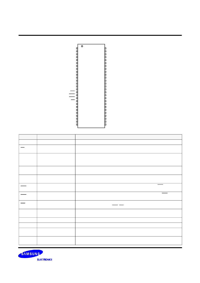
PIN CONFIGURATION
(Top view)
V
SS
N.C
V
SSQ
N.C
DQ3
V
DDQ
N.C
N.C
V
SSQ
N.C
DQ2
V
DDQ
N.C
V
SS
N.C/RFU
DQM
CLK
CKE
N.C
A11
A9
A8
A7
A6
A5
A4
V
SS
54Pin TSOP (II)
(400mil x 875mil)
(0.8 mm Pin pitch)
PIN FUNCTION DESCRIPTION
Pin
Name
Input Function
CLK
System clock
Active on the positive going edge to sample all inputs.
CS
Chip select
Disables or enables device operation by masking or enabling all inputs except
CLK, CKE and DQM
CKE
Clock enable
Masks system clock to freeze operation from the next clock cycle.
CKE should be enabled at least one cycle prior to new command.
Disable input buffers for power down in standby.
A
0
~ A
12
Address
Row/column addresses are multiplexed on the same pins.
Row address : RA
0
~ RA
12
, Column address : CA
0
~ CA
9
BA
Bank select address
Selects bank to be activated during row address latch time.
Selects bank for read/write during column address latch time.
RAS
Row address strobe
Latches row addresses on the positive going edge of the CLK with RAS low.
Enables row access & precharge.
CAS
Column address strobe
Latches column addresses on the positive going edge of the CLK with CAS low.
Enables column access.
WE
Write enable
Enables write operation and row precharge.
Latches data in starting from CAS, WE active.
DQM
Data input/output mask
Makes data output Hi-Z, t
SHZ
after the clock and masks the output.
Blocks data input when DQM active.
DQ
0
~
3
Data input/output
Data inputs/outputs are multiplexed on the same pins.
V
DD
/V
SS
Power supply/ground
Power and ground for the input buffers and the core logic.
V
DDQ
/V
SSQ
Data output power/ground
Isolated power supply and ground for the output buffers to provide improved noise
immunity.
N.C/RFU
No connection
/reserved for future use
This pin is recommended to be left No Connection on the device.
相關(guān)PDF資料 |
PDF描述 |
|---|---|
| KM44S4020CT | 2M x 4Bit x 2 Banks Synchronous DRAM(2M x 4位 x 2組同步動(dòng)態(tài)RAM) |
| KM44S64230A | 16M x 4Bit x 4 Banks Synchronous DRAM(16M x 4位 x 4組同步動(dòng)態(tài)RAM) |
| KM44V1000D | 1M x 4Bit CMOS Dynamic RAM with Fast Page Mode(1M x 4位CMOS 動(dòng)態(tài)RAM(帶快速頁(yè)模式)) |
| KM44V16000B | 16M x 4Bit CMOS Dynamic RAM with Fast Page Mode(16M x 4位CMOS 動(dòng)態(tài)RAM(帶快速頁(yè)模式)) |
| KM44V16100B | 16M x 4Bit CMOS Dynamic RAM with Fast Page Mode(16M x 4位CMOS 動(dòng)態(tài)RAM(帶快速頁(yè)模式)) |
相關(guān)代理商/技術(shù)參數(shù) |
參數(shù)描述 |
|---|---|
| KM44S16020CT-G10 | 制造商:SEC 功能描述: |
| KM44S32030 | 制造商:SAMSUNG 制造商全稱(chēng):Samsung semiconductor 功能描述:8M x 4Bit x 4 Banks Synchronous DRAM |
| KM44S32030B | 制造商:SAMSUNG 制造商全稱(chēng):Samsung semiconductor 功能描述:128Mbit SDRAM 8M x 4Bit x 4 Banks Synchronous DRAM LVTTL |
| KM44S32030BT-G/F10 | 制造商:SAMSUNG 制造商全稱(chēng):Samsung semiconductor 功能描述:128Mbit SDRAM 8M x 4Bit x 4 Banks Synchronous DRAM LVTTL |
| KM44S32030BT-G/F8 | 制造商:SAMSUNG 制造商全稱(chēng):Samsung semiconductor 功能描述:128Mbit SDRAM 8M x 4Bit x 4 Banks Synchronous DRAM LVTTL |
發(fā)布緊急采購(gòu),3分鐘左右您將得到回復(fù)。