- 您現(xiàn)在的位置:買賣IC網(wǎng) > PDF目錄30731 > LC72715PW (SANYO SEMICONDUCTOR CO LTD) SPECIALTY CONSUMER CIRCUIT, PQFP64 PDF資料下載
參數(shù)資料
| 型號(hào): | LC72715PW |
| 廠商: | SANYO SEMICONDUCTOR CO LTD |
| 元件分類: | 消費(fèi)家電 |
| 英文描述: | SPECIALTY CONSUMER CIRCUIT, PQFP64 |
| 封裝: | 10 X 10 MM, SQFP-64 |
| 文件頁數(shù): | 4/26頁 |
| 文件大小: | 167K |
| 代理商: | LC72715PW |
第1頁第2頁第3頁當(dāng)前第4頁第5頁第6頁第7頁第8頁第9頁第10頁第11頁第12頁第13頁第14頁第15頁第16頁第17頁第18頁第19頁第20頁第21頁第22頁第23頁第24頁第25頁第26頁

LC72715PW
No.A1650-12/26
(3) Corrected data output
This is to output the packet data after correction processing from LSI. The total length of output data is 176 bits (22
Bytes) only, and the Layer 2 CRC data (14 bits) and parity data (82 bits) are not output. The corrected data is output,
on either the 8-bit or 16-bit units, sequentially from the leading data among those in one packet. The BIC code is not
output.
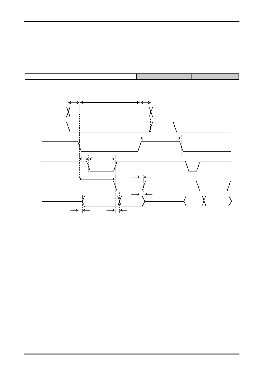
The accessing method is the same as for the register output and the address “0” is input to A0 to A3 pins. Since this
is different from the register output in the timing conditions during access, the timing chart is shown here separately
from the register output. The RDY signal output method can also be selected similarly.
Data block (176 bits) Data after error correction
Layer 2 CRC (14 bits)
Parity (82 bits)
Structure of a Single Data Packet (Total length 272 bits: BIC not included)
(4) Layer 4 CRC check output
This is a function to detect error of data group (layer 4 CRC). The CRC4 pin = “H” or bit1 (CRC4) = 1 of the status
register after writing of the data group into the layer 4 CRC register means that there is no error. The accessing
method is the same as for the data input, and the address “6h” of the layer 4 CRC register is input into the register
address.
(5) DMA transmission output
Setting bit0 (DMA) = 1 of control register 2 causes the DMA mode, allowing the corrected data to be output in the
DMA method.
For accessing, input the address “0h” to A0 to A3 pins after falling of the DREQ output pin, setting the CS pin = L,
and then the RD pin = L. After the DREQ pin = H, data is acquired from the D(n) pin. Then, the wait state occurs for
the tCYDM period or longer till the DREQ pin becomes “L”. In the DMA mode, only 8 bits can be selected for the
data bus width. (n: 0 to 7 for BUSWD=L. Do not set BUSWD=H because it may cause fault.)
The DACK pin can be used instead of the RD pin for DMA transmission. In this case, it is necessary to set bit1
(DMA_RD) = 1 of the control register 2. It is also possible to change the polarity of DREQ and DACK pins. In this
case, it is necessary to set bit4 (DREQ) = 1 and bit5 (DACK) = 1 of the control register 2.
tSARD
tHARD
tRDH
tWDRD
tCYRD
A0 to A3
CS
RD
D(n)
VALID
OUTPUT
RDY (Timing1: default)
tWDRDY
tDRDY
RDY (Timing2)
VALID
OUTPUT
tDDATn
* A0 to A3 should be set to 0 during
reading of corrected data.
tDRDY2
tDATON
tDRDY+tWRDY
相關(guān)PDF資料 |
PDF描述 |
|---|---|
| LC72720NM | SPECIALTY CONSUMER CIRCUIT, PDSO24 |
| LC72720NM | SPECIALTY CONSUMER CIRCUIT, PDSO24 |
| LC72720N | SPECIALTY CONSUMER CIRCUIT, PDIP24 |
| LC72720N | SPECIALTY CONSUMER CIRCUIT, PDIP24 |
| LC72720YV | SPECIALTY CONSUMER CIRCUIT, PDSO30 |
相關(guān)代理商/技術(shù)參數(shù) |
參數(shù)描述 |
|---|---|
| LC72717PW | 制造商:SANYO 制造商全稱:Sanyo Semicon Device 功能描述:Mobile FM Multiplex Broadcast (DARC) Receiver IC |
| LC72720 | 制造商:SANYO 制造商全稱:Sanyo Semicon Device 功能描述:Single-Chip RDS Signal-Processing System LSI |
| LC72720M | 制造商:SANYO 制造商全稱:Sanyo Semicon Device 功能描述:Single-Chip RDS Signal-Processing System LSI |
| LC72720N | 制造商:SANYO 制造商全稱:Sanyo Semicon Device 功能描述:Single-Chip RDS Signal-Processing System LSI |
| LC72720NM | 制造商:SANYO 制造商全稱:Sanyo Semicon Device 功能描述:Single-Chip RDS Signal-Processing System LSI |
發(fā)布緊急采購,3分鐘左右您將得到回復(fù)。