- 您現(xiàn)在的位置:買賣IC網(wǎng) > PDF目錄370992 > M66287FP (Mitsubishi Electric Corporation) 262144-word x 8-bit x 3-FIELD MEMORY PDF資料下載
參數(shù)資料
| 型號: | M66287FP |
| 廠商: | Mitsubishi Electric Corporation |
| 英文描述: | 262144-word x 8-bit x 3-FIELD MEMORY |
| 中文描述: | 262144字× 8位× 3場記憶 |
| 文件頁數(shù): | 1/21頁 |
| 文件大?。?/td> | 196K |
| 代理商: | M66287FP |

MITSUBISHI <DIGITAL ASSP>
M66287FP
262144-word x 8-bit x 3-FIELD MEMORY
2002 MITSUBISHI ELECTRIC CORPORATION
1
DESCRIPTION
The M66287FP is a high-speed field memory with three FIFO (First In First Out) memories of 262144-word x 8-bit
configuration (2M bits) which uses high-performance silicon gate CMOS process technology. One of three FIFO memories
consists of two FIFO memories of 262144-word x 4-bit (1M bits). Five types of operation can be performed through the
following mode settings:
Mode1 : 3-system delay data output by 3-system individual input of 256K-word x 8-bit FIFO
Mode2 : Simultaneous output of 1 to 3-line delay data by 1-system input of 256K-word x 8-bit FIFO
Mode3 : Simultaneous output of 1 to 2-line delay data by 1-system input of 256K-word x 8-bit FIFO
and,1-system delay data output by 1-system input of 256K-word x 8-bit FIFO
Mode4 : 2-system delay data output by 2-system individual input of 256K-word x 12-bit FIFO
Mode5 : Simultaneous output of 1 to 2-line delay data by 1-system input of 256K-word x 12-bit FIFO
The above-mentioned function is most suitable for image data correction across multiple fields. Because three pieces of
2M-bit FIFO are contained in one chip, a low power consumption of a set can be realized.
FEATURES
z
Memory configuration
The total memory capacity is 6M bits (static memory).
The following two types of memory configurations can be selected.
262144-word x 8-bit x 3-line configuration
262144-word x 12-bit x 2-line configuration
16.6 ns (Min.)
13.0 ns (Max.)
2.0 ns (Min.)
Internal = 1.8 V ± 0.18 V
I/O = 3.3 V ± 0.3 V
z
High - speed cycle
z
High - speed access
z
Output hold
z
Supply voltage
z
Variable length delay bit
z
Five modes can be selected
z
Write and read function can be operated completely independently and asynchronously
z
Output
3 states
z
Package
100pin QFP (100P6Q-A)
APPLICATION
W-CDMA base station, Digital PPC, Digital television, VTR and so on.
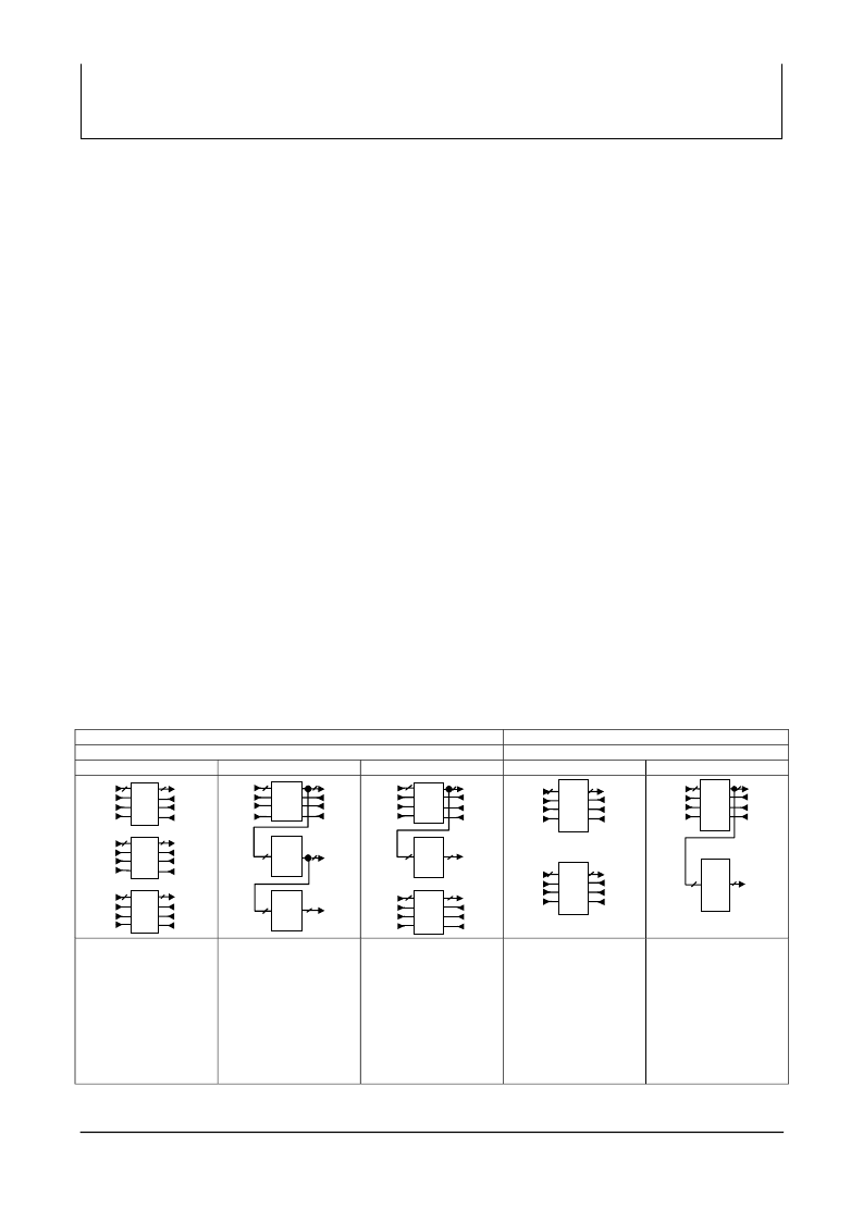
MODE DESCRIPTIONS DRAWING
2M-bit x 3 configuration
8-bit bus I/F
MODE 2
3M-bit x 2 configuration
12-bit bus I/F
MODE 4
MODE 1
MODE 3
MODE 5
8
DA<7:0>
WCKA
WRESA
WEA
8
x
8-bit
QA<7:0>
RCKA
RRESA
REA
8
DB<7:0>
WCKB
WRESB
WEB
8
QB<7:0>
RCKB
RRESB
REB
x
8-bit
8
DC<7:0>
WCKC
WRESC
WEC
8
QC<7:0>
RCKC
RRESC
REC
x
8-bit
8
8
8
8
8
8
2x
8-bit
2x
8-bit
2x
8-bit
DA<7:0>
WCKA
WRESA
WEA
QB<7:0>
QC<7:0>
QA<7:0>
RCKA
RRESA
REA
8
8
8
8
2x
8-bit
2x
8-bit
8
8
2x
8-bit
DA<7:0>
WCKA
WRESA
WEA
QA<7:0>
RCKA
RRESA
REA
QB<7:0>
QC<7:0>
RCKC
RRESC
REC
DC<7:0>
WCKC
WRESC
WEC
12
x
12-bit
12
DA<11:0>
WCKA
WRESA
WEA
QA<11:0>
RCKA
RRESA
REA
DB<11:0>
WCKB
WRESB
WEB
QB<11:0>
RCKB
RRESB
REB
12
x
12-bit
12
12
2x
12-bit
x
12-bit
12
12
12
DA<11:0>
WCKA
WRESA
WEA
QA<11:0>
RCKA
RRESA
REA
QB<11:0>
The three pieces of 256K-
word x 8-bit FIFO can be
operated completely
independently.
The three pieces of 256K-
word x 8-bit FIFO are
cascade-connected.
Write and read operation
of FIFO after the 2nd line
is controlled by the read
system pin of the 1st line.
The two pieces of 256K-
word x 8-bit FIFO are
cascade-connected and, a
piece of 256K-word x 8-bit
FIFO can be operated
completely independently.
Write and read operation
of FIFO at the 2nd line is
controlled by the read
system pin of the 1st line.
The two pieces of 256K-
word x 12-bit FIFO can be
operated completely
independently.
The two pieces of 256K-
word x 12-bit FIFO are
cascade-connected.
Write and read operation
of FIFO at the 2nd line is
controlled by the read
system pin of the 1st line.
Note: Please refer to “Pin Assignment Table” in “MODE 4 and MODE 5 OPERATION DESCRIPTIONS” for
assignment of external pins, Dx<11:0> and Qx<11:0> when used in 12-bit bus interface.
相關PDF資料 |
PDF描述 |
|---|---|
| M66307FP | LINE SCAN BUFFER with 16-BIT MPU BUS COMPATIBLE INPUTS |
| M66307SP | LINE SCAN BUFFER with 16-BIT MPU BUS COMPATIBLE INPUTS |
| M66312FP | 16-BIT LED DRIVER WITH SHIFT REGISTER AND LATCHED 3-STATE OUTPUTS |
| M66312P | 16-BIT LED DRIVER WITH SHIFT REGISTER AND LATCHED 3-STATE OUTPUTS |
| M66313FP | 32-BIT LED DRIVER WITH SHIFT REGISTER AND LATCH |
相關代理商/技術參數(shù) |
參數(shù)描述 |
|---|---|
| M66288FP | 制造商:RENESAS 制造商全稱:Renesas Technology Corp 功能描述:262144-word x 8-bit x 3-FIFO MEMORY |
| M66290AFP | 制造商:RENESAS 制造商全稱:Renesas Technology Corp 功能描述:USB DEVICE CONTROLLER |
| M66290AGP | 制造商:RENESAS 制造商全稱:Renesas Technology Corp 功能描述:USB DEVICE CONTROLLER |
| M66291GP | 制造商:Renesas Electronics Corporation 功能描述: |
| M66291GP#201 | 制造商:Renesas Electronics Corporation 功能描述:IC ASSP USB2.0 DEVICE CONTROLLER 48LQFP |
發(fā)布緊急采購,3分鐘左右您將得到回復。