- 您現(xiàn)在的位置:買(mǎi)賣(mài)IC網(wǎng) > PDF目錄370992 > M66287FP (Mitsubishi Electric Corporation) 262144-word x 8-bit x 3-FIELD MEMORY PDF資料下載
參數(shù)資料
| 型號(hào): | M66287FP |
| 廠商: | Mitsubishi Electric Corporation |
| 英文描述: | 262144-word x 8-bit x 3-FIELD MEMORY |
| 中文描述: | 262144字× 8位× 3場(chǎng)記憶 |
| 文件頁(yè)數(shù): | 8/21頁(yè) |
| 文件大小: | 196K |
| 代理商: | M66287FP |
第1頁(yè)第2頁(yè)第3頁(yè)第4頁(yè)第5頁(yè)第6頁(yè)第7頁(yè)當(dāng)前第8頁(yè)第9頁(yè)第10頁(yè)第11頁(yè)第12頁(yè)第13頁(yè)第14頁(yè)第15頁(yè)第16頁(yè)第17頁(yè)第18頁(yè)第19頁(yè)第20頁(yè)第21頁(yè)

MITSUBISHI <DIGITAL ASSP>
M66287FP
262144-word x 8-bit x 3-FIELD MEMORY
2002 MITSUBISHI ELECTRIC CORPORATION
8
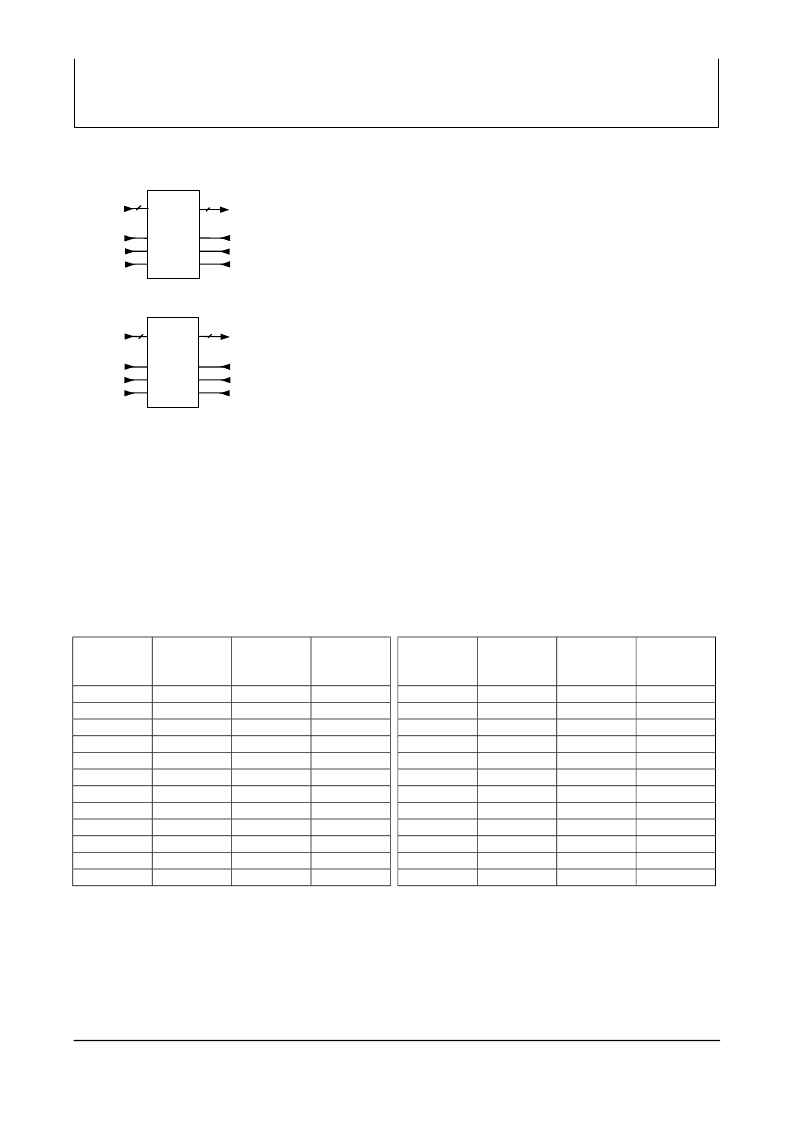
MODE 4 OPERATION DESCRIPTIONS
<Mode 4>
In mode 4, two FIFO memories with 12-bit data bus can be controlled completely
individually. Taking FIFO (A) as an example, the operation of FIFO memory is
described below. The operation of FIFO (B) is the same as that of FIFO (A).
When write enable input WEA is "L", the contents of data input DA<7:0> and
DB<3:0>are written into FIFO (A) in synchronization with the rising of write clock
input WCKA. At this time, the write address counter of FIFO (A) is incremented.
When WEA is "H", writing into FIFO (A) is disabled and the write address counter
of FIFO (A) is stopped.
When write reset input WRESA is "L", the write address counter of FIFO (A) is
initialized.
When read enable input REA is "L", the contents of FIFO (A) are outputted to data output QA<7:0> and QB<3:0> in
synchronization with the rising of read clock input RCKA. At this time, the read address counter of FIFO (A) is incremented.
When REA is "H", reading from FIFO (A) is disabled and the read address counter of FIFO (A) is stopped. Also QA<7:0>
and QB<3:0> become high impedance state.
When read reset input RRESA is "L", the read address counter of FIFO (A) is initialized.
Also, set the 12-bit I/O buses of FIFO (A) and FIFO (B) as shown in the table below.
In mode 4, all pins for the A-system and B-system, DC<7:0> and QC<7:0> are only used. Therefore the write/read control
pins for the C-system should be fixed at "L" or "H".
External pin
name
Data
bus of FIFO
(A)
11-bit
10-bit
9-bit
8-bit
7-bit
6-bit
5-bit
4-bit
3-bit
2-bit
1-bit
0-bit
input
External pin
name
Data output
bus of FIFO
(A)
11-bit
10-bit
9-bit
8-bit
7-bit
6-bit
5-bit
4-bit
3-bit
2-bit
1-bit
0-bit
External pin
name
Data
bus of FIFO
(B)
11-bit
10-bit
9-bit
8-bit
7-bit
6-bit
5-bit
4-bit
3-bit
2-bit
1-bit
0-bit
input
External pin
name
Data output
bus of FIFO
(B)
11-bit
10-bit
9-bit
8-bit
7-bit
6-bit
5-bit
4-bit
3-bit
2-bit
1-bit
0-bit
DA<7>
DA<6>
DA<5>
DA<4>
DA<3>
DA<2>
DA<1>
DA<0>
DB<3>
DB<2>
DB<1>
DB<0>
QA<7>
QA<6>
QA<5>
QA<4>
QA<3>
QA<2>
QA<1>
QA<0>
QB<3>
QB<2>
QB<1>
QB<0>
DC<7>
DC<6>
DC<5>
DC<4>
DC<3>
DC<2>
DC<1>
DC<0>
DB<7>
DB<6>
DB<5>
DB<4>
QC<7>
QC<6>
QC<5>
QC<4>
QC<3>
QC<2>
QC<1>
QC<0>
QB<7>
QB<6>
QB<5>
QB<4>
Note : The two pieces of 256K-word x 12-bit FIFO can be operated completely independently.
DA<7:0>
DB<3:0>
WCKA
WRESA
WEA
12
12
256K
x
12-bit
FIFO(A)
QA<7:0>
QB<3:0>
256K
x
12-bit
FIFO(B)
12
12
QC<7:0>
QB<7:4>
DB<7:4>
WCKB
WRESB
WEB
DC<7:0>
RCKB
RRESB
REB
RCKA
RRESA
REA
相關(guān)PDF資料 |
PDF描述 |
|---|---|
| M66307FP | LINE SCAN BUFFER with 16-BIT MPU BUS COMPATIBLE INPUTS |
| M66307SP | LINE SCAN BUFFER with 16-BIT MPU BUS COMPATIBLE INPUTS |
| M66312FP | 16-BIT LED DRIVER WITH SHIFT REGISTER AND LATCHED 3-STATE OUTPUTS |
| M66312P | 16-BIT LED DRIVER WITH SHIFT REGISTER AND LATCHED 3-STATE OUTPUTS |
| M66313FP | 32-BIT LED DRIVER WITH SHIFT REGISTER AND LATCH |
相關(guān)代理商/技術(shù)參數(shù) |
參數(shù)描述 |
|---|---|
| M66288FP | 制造商:RENESAS 制造商全稱:Renesas Technology Corp 功能描述:262144-word x 8-bit x 3-FIFO MEMORY |
| M66290AFP | 制造商:RENESAS 制造商全稱:Renesas Technology Corp 功能描述:USB DEVICE CONTROLLER |
| M66290AGP | 制造商:RENESAS 制造商全稱:Renesas Technology Corp 功能描述:USB DEVICE CONTROLLER |
| M66291GP | 制造商:Renesas Electronics Corporation 功能描述: |
| M66291GP#201 | 制造商:Renesas Electronics Corporation 功能描述:IC ASSP USB2.0 DEVICE CONTROLLER 48LQFP |
發(fā)布緊急采購(gòu),3分鐘左右您將得到回復(fù)。