- 您現(xiàn)在的位置:買賣IC網(wǎng) > PDF目錄370992 > M66287FP (Mitsubishi Electric Corporation) 262144-word x 8-bit x 3-FIELD MEMORY PDF資料下載
參數(shù)資料
| 型號(hào): | M66287FP |
| 廠商: | Mitsubishi Electric Corporation |
| 英文描述: | 262144-word x 8-bit x 3-FIELD MEMORY |
| 中文描述: | 262144字× 8位× 3場記憶 |
| 文件頁數(shù): | 7/21頁 |
| 文件大?。?/td> | 196K |
| 代理商: | M66287FP |

MITSUBISHI <DIGITAL ASSP>
M66287FP
262144-word x 8-bit x 3-FIELD MEMORY
2002 MITSUBISHI ELECTRIC CORPORATION
7
MODE 3 OPERATION DESCRIPTIONS
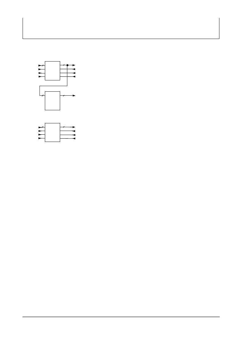
<Mode 3>
In mode 3, two FIFO memories with 8-bit data bus are cascade-connected
and the other FIFO memory with an 8-bit data bus is configured completely
independently. This makes it possible to generate delay data for 2-lines
without external wiring and to control the other independent one FIFO
memory.
When write enable input WEA is "L", the contents of data input DA<7:0> are
written into FIFO (A) in synchronization with the rising of write clock input
WCKA. At this time, the write address counter of FIFO (A) is incremented.
When WEA is "H", writing into FIFO (A) is disabled and the write address
counter of FIFO (A) is stopped.
When write reset input WRESA is "L", the write address counter of FIFO (A) is
initialized.
When read enable input REA is "L", the contents of FIFO (A) and FIFO (B) are
outputted to each QA<7:0> and QB<7:0> in synchronization with the rising of
read clock input RCKA. At this time, the read address counters of FIFO (A)
and FIFO (B) are incremented.
Also the data of FIFO (A) is written into FIFO (B) in synchronization with the rising of RCKA. At this time, the write address
counter of FIFO (B) is incremented simultaneously.
When REA is "H", reading from FIFO (A) and FIFO (B) is disabled and the read address counter of each FIFO is stopped.
Also QA<7:0> and QB<7:0> become high impedance state. And writing into FIFO (B) is disabled and the write address
counter of FIFO (B) is stopped.
When read reset input RRESA is "L", the read address counter of FIFO (A) and the write address counter/read address
counter of FIFO (B) are initialized.
The operation of FIFO (C) is the same as that of mode 1.
And, in mode 3, all pins for the A-system and C-system, and QB<7:0> are only used. Therefore the write/read control pins
for the B-system and DB<7:0> should be fixed at "L" or "H".
Note : The two pieces of 256K-word x 8-bit FIFO are cascade-connected and, a piece of 256K-word x 8-bit FIFO
can be operated completely independently.
Write and read operation of FIFO at the 2nd line is controlled by the read system pin of the 1st line.
DA<7:0>
WCKA
WRESA
WEA
8
8
256K
x
8-bit
FIFO(A)
QA<7:0>
RCKA
RRESA
REA
QB<7:0>
8
256K
x
8-bit
FIFO(B)
8
DC<7:0>
WCKC
WRESC
WEC
QC<7:0>
RCKC
RRESC
REC
8
256K
x
8-bit
FIFO(C)
8
相關(guān)PDF資料 |
PDF描述 |
|---|---|
| M66307FP | LINE SCAN BUFFER with 16-BIT MPU BUS COMPATIBLE INPUTS |
| M66307SP | LINE SCAN BUFFER with 16-BIT MPU BUS COMPATIBLE INPUTS |
| M66312FP | 16-BIT LED DRIVER WITH SHIFT REGISTER AND LATCHED 3-STATE OUTPUTS |
| M66312P | 16-BIT LED DRIVER WITH SHIFT REGISTER AND LATCHED 3-STATE OUTPUTS |
| M66313FP | 32-BIT LED DRIVER WITH SHIFT REGISTER AND LATCH |
相關(guān)代理商/技術(shù)參數(shù) |
參數(shù)描述 |
|---|---|
| M66288FP | 制造商:RENESAS 制造商全稱:Renesas Technology Corp 功能描述:262144-word x 8-bit x 3-FIFO MEMORY |
| M66290AFP | 制造商:RENESAS 制造商全稱:Renesas Technology Corp 功能描述:USB DEVICE CONTROLLER |
| M66290AGP | 制造商:RENESAS 制造商全稱:Renesas Technology Corp 功能描述:USB DEVICE CONTROLLER |
| M66291GP | 制造商:Renesas Electronics Corporation 功能描述: |
| M66291GP#201 | 制造商:Renesas Electronics Corporation 功能描述:IC ASSP USB2.0 DEVICE CONTROLLER 48LQFP |
發(fā)布緊急采購,3分鐘左右您將得到回復(fù)。