- 您現(xiàn)在的位置:買賣IC網(wǎng) > PDF目錄69030 > MC94MX21DVKN3R2 (FREESCALE SEMICONDUCTOR INC) 350 MHz, MICROPROCESSOR, PBGA289 PDF資料下載
參數(shù)資料
| 型號: | MC94MX21DVKN3R2 |
| 廠商: | FREESCALE SEMICONDUCTOR INC |
| 元件分類: | 微控制器/微處理器 |
| 英文描述: | 350 MHz, MICROPROCESSOR, PBGA289 |
| 封裝: | 14 X 14 MM, 1.41 MM HEIGHT, 0.65 MM PITCH, LEAD FREE, PLASTIC, BGA-289 |
| 文件頁數(shù): | 49/98頁 |
| 文件大小: | 1326K |
| 代理商: | MC94MX21DVKN3R2 |
第1頁第2頁第3頁第4頁第5頁第6頁第7頁第8頁第9頁第10頁第11頁第12頁第13頁第14頁第15頁第16頁第17頁第18頁第19頁第20頁第21頁第22頁第23頁第24頁第25頁第26頁第27頁第28頁第29頁第30頁第31頁第32頁第33頁第34頁第35頁第36頁第37頁第38頁第39頁第40頁第41頁第42頁第43頁第44頁第45頁第46頁第47頁第48頁當前第49頁第50頁第51頁第52頁第53頁第54頁第55頁第56頁第57頁第58頁第59頁第60頁第61頁第62頁第63頁第64頁第65頁第66頁第67頁第68頁第69頁第70頁第71頁第72頁第73頁第74頁第75頁第76頁第77頁第78頁第79頁第80頁第81頁第82頁第83頁第84頁第85頁第86頁第87頁第88頁第89頁第90頁第91頁第92頁第93頁第94頁第95頁第96頁第97頁第98頁
Specifications
MC94MX21 Technical Data, Rev. 1.
Freescale Semiconductor
53
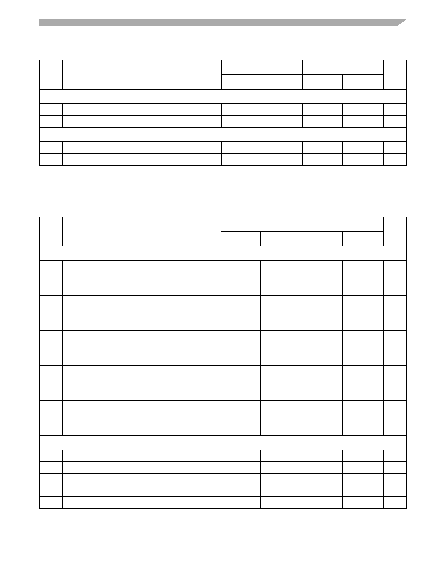
Synchronous Internal Clock Operation (SAP Ports)
31
SRXD setup before (Tx) CK falling
23.00
–
21.41
–
ns
32
SRXD hold after (Tx) CK falling
0
–
0
–
ns
Synchronous External Clock Operation (SAP Ports)
33
SRXD setup before (Tx) CK falling
1.20
–
0.88
–
ns
34
SRXD hold after (Tx) CK falling
0
–
0
–
ns
1. All the timings for the SSI are given for a non-inverted serial clock polarity (TSCKP/RSCKP = 0) and a non-inverted frame sync
(TFSI/RFSI = 0). If the polarity of the clock and/or the frame sync have been inverted, all the timing remains valid by inverting
the clock signal STCK/SRCK and/or the frame sync STFS/SRFS shown in the tables and in the figures.
Table 34. SSI to SSI1 Ports Timing Parameters
Ref
No.
Parameter
1.8 V
± 0.1 V
3.0 V
± 0.3 V
Unit
Minimum
Maximum
Minimum
Maximum
Internal Clock Operation1 (SSI1 Ports)
1
(Tx/Rx) CK clock period1
90.91
–
90.91
–
ns
2
(Tx) CK high to FS (bl) high
-0.68
-0.15
-0.68
-0.15
ns
3
(Rx) CK high to FS (bl) high
-0.96
-0.27
-0.96
-0.27
ns
4
(Tx) CK high to FS (bl) low
-0.68
-0.15
-0.68
-0.15
ns
5
(Rx) CK high to FS (bl) low
-0.96
-0.27
-0.96
-0.27
ns
6
(Tx) CK high to FS (wl) high
-0.68
-0.15
-0.68
-0.15
ns
7
(Rx) CK high to FS (wl) high
-0.96
-0.27
-0.96
-0.27
ns
8
(Tx) CK high to FS (wl) low
-0.68
-0.15
-0.68
-0.15
ns
9
(Rx) CK high to FS (wl) low
-0.96
-0.27
-0.96
-0.27
ns
10
(Tx) CK high to STXD valid from high impedance
-1.68
-0.36
-1.68
-0.36
ns
11a
(Tx) CK high to STXD high
-1.68
-0.36
-1.68
-0.36
ns
11b
(Tx) CK high to STXD low
-1.68
-0.36
-1.68
-0.36
ns
12
(Tx) CK high to STXD high impedance
-1.58
-0.31
-1.58
-0.31
ns
13
SRXD setup time before (Rx) CK low
20.41
–
20.41
–
ns
14
SRXD hold time after (Rx) CK low
0
–
0
–
ns
External Clock Operation (SSI1 Ports)
15
(Tx/Rx) CK clock period1
90.91
–
90.91
–
ns
16
(Tx/Rx) CK clock high period
36.36
–
36.36
–
ns
17
(Tx/Rx) CK clock low period
36.36
–
36.36
–
ns
18
(Tx) CK high to FS (bl) high
10.22
17.63
8.82
16.24
ns
19
(Rx) CK high to FS (bl) high
10.79
19.67
9.39
18.28
ns
Table 33. SSI to SAP Ports Timing Parameters (Continued)
Ref
No.
Parameter
1.8 V
± 0.1 V
3.0 V
± 0.3 V
Unit
Minimum
Maximum
Minimum
Maximum
Because
of
an
order
from
the
United
States
International
Trade
Commission,
BGA-packaged
product
lines
and
part
numbers
indicated
here
currently
are
not
available
from
Freescale
for
import
or
sale
in
the
United
States
prior
to
September
2010:
MC94MX21DVKN3
相關(guān)PDF資料 |
PDF描述 |
|---|---|
| MC9S08FL8CLC | 8-BIT, FLASH, 20 MHz, MICROCONTROLLER, QFP32 |
| MC9S08FL8CBM | 8-BIT, FLASH, 20 MHz, MICROCONTROLLER, PDIP32 |
| MC9S08FL16CBM | 8-BIT, FLASH, 20 MHz, MICROCONTROLLER, PDIP32 |
| MC9S08GW64CLH | MICROCONTROLLER, PQFP64 |
| MC9S08GW64CLK | MICROCONTROLLER, PQFP80 |
相關(guān)代理商/技術(shù)參數(shù) |
參數(shù)描述 |
|---|---|
| MC94MX21DVKN3R2 | 制造商:Freescale Semiconductor 功能描述:32-bit Embedded Microprocessors |
| MC950 | 制造商:FREESCALE 制造商全稱:Freescale Semiconductor, Inc 功能描述:INTEGRATED CIRCUITS |
| MC951 | 制造商:FREESCALE 制造商全稱:Freescale Semiconductor, Inc 功能描述:INTEGRATED CIRCUITS |
| MC952 | 制造商:FREESCALE 制造商全稱:Freescale Semiconductor, Inc 功能描述:INTEGRATED CIRCUITS |
| MC953 | 制造商:MOTOROLA 制造商全稱:Motorola, Inc 功能描述:INTEGRATED CIRCUITS |
發(fā)布緊急采購,3分鐘左右您將得到回復(fù)。