- 您現(xiàn)在的位置:買賣IC網(wǎng) > PDF目錄69030 > MC94MX21DVKN3R2 (FREESCALE SEMICONDUCTOR INC) 350 MHz, MICROPROCESSOR, PBGA289 PDF資料下載
參數(shù)資料
| 型號(hào): | MC94MX21DVKN3R2 |
| 廠商: | FREESCALE SEMICONDUCTOR INC |
| 元件分類: | 微控制器/微處理器 |
| 英文描述: | 350 MHz, MICROPROCESSOR, PBGA289 |
| 封裝: | 14 X 14 MM, 1.41 MM HEIGHT, 0.65 MM PITCH, LEAD FREE, PLASTIC, BGA-289 |
| 文件頁(yè)數(shù): | 56/98頁(yè) |
| 文件大?。?/td> | 1326K |
| 代理商: | MC94MX21DVKN3R2 |
第1頁(yè)第2頁(yè)第3頁(yè)第4頁(yè)第5頁(yè)第6頁(yè)第7頁(yè)第8頁(yè)第9頁(yè)第10頁(yè)第11頁(yè)第12頁(yè)第13頁(yè)第14頁(yè)第15頁(yè)第16頁(yè)第17頁(yè)第18頁(yè)第19頁(yè)第20頁(yè)第21頁(yè)第22頁(yè)第23頁(yè)第24頁(yè)第25頁(yè)第26頁(yè)第27頁(yè)第28頁(yè)第29頁(yè)第30頁(yè)第31頁(yè)第32頁(yè)第33頁(yè)第34頁(yè)第35頁(yè)第36頁(yè)第37頁(yè)第38頁(yè)第39頁(yè)第40頁(yè)第41頁(yè)第42頁(yè)第43頁(yè)第44頁(yè)第45頁(yè)第46頁(yè)第47頁(yè)第48頁(yè)第49頁(yè)第50頁(yè)第51頁(yè)第52頁(yè)第53頁(yè)第54頁(yè)第55頁(yè)當(dāng)前第56頁(yè)第57頁(yè)第58頁(yè)第59頁(yè)第60頁(yè)第61頁(yè)第62頁(yè)第63頁(yè)第64頁(yè)第65頁(yè)第66頁(yè)第67頁(yè)第68頁(yè)第69頁(yè)第70頁(yè)第71頁(yè)第72頁(yè)第73頁(yè)第74頁(yè)第75頁(yè)第76頁(yè)第77頁(yè)第78頁(yè)第79頁(yè)第80頁(yè)第81頁(yè)第82頁(yè)第83頁(yè)第84頁(yè)第85頁(yè)第86頁(yè)第87頁(yè)第88頁(yè)第89頁(yè)第90頁(yè)第91頁(yè)第92頁(yè)第93頁(yè)第94頁(yè)第95頁(yè)第96頁(yè)第97頁(yè)第98頁(yè)
MC94MX21 Technical Data, Rev. 1.
5
6
Freescale Semiconductor
Signal Descriptions
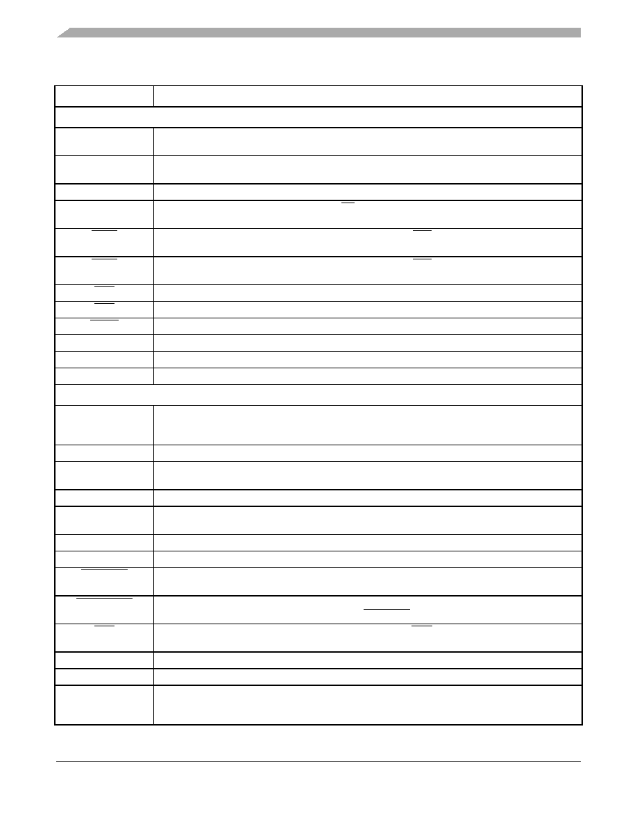
SDRAM Controller
SDBA [4:0]
SDRAM non-interleave mode bank address signals. These signals are multiplexed with address signals
A[20:16].
SDIBA [3:0]
SDRAM interleave addressing mode bank address signals. These signals are multiplexed with address
signals A[24:21].
MA [11:0]
SDRAM address signals. MA[9:0] are multiplexed with address signals A[10:1].
DQM [3:0]
SDRAM data qualifier mask multiplexed with EB[3:0]. DQM3 corresponds to D[31:24], DQM2
corresponds to D[23:16], DQM1 corresponds to D[15:8], and DQM0 corresponds to D[7:0].
CSD0
SDRAM Chip Select signal. This signal is multiplexed with the CS2 signal. This signal is selectable by
programming the Function Multiplexing Control Register in the System Control chapter.
CSD1
SDRAM Chip Select signal. This signal is multiplexed with the CS3 signal. This signal is selectable by
programming the Function Multiplexing Control Register in the System Control chapter.
RAS
SDRAM Row Address Select signal.
CAS
SDRAM Column Address Select signal
SDWE
SDRAM Write Enable signal
SDCKE0
SDRAM Clock Enable 0
SDCKE1
SDRAM Clock Enable 1
SDCLK
SDRAM Clock
Clocks and Resets
EXTAL26M
Crystal input (26MHz), or a 16 MHz to 32 MHz oscillator (or square-wave) input when the internal
oscillator circuit is shut down. When using an external signal source, feed this input with a square wave
signal switching from GND to VDDA.
XTAL26M
Oscillator output to external crystal. When using an external signal source, float this output.
EXTAL32K
32 kHz or 32.768 kHz crystal input. When using an external signal source, feed this input with a square
wave signal switching from GND to QVDD5.
XTAL32K
Oscillator output to external crystal. When using an external signal source, float this output.
CLKO
Clock Out signal selected from internal clock signals. Please refer to clock controller for internal clock
selection.
EXT_48M
This is a special factory test signal. To ensure proper operation, connect this signal to ground.
EXT_266M
This is a special factory test signal. To ensure proper operation, connect this signal to ground.
RESET_IN
Master Reset—External active low Schmitt trigger input signal. When this signal goes active, all modules
(except the reset module, SDRAMC module, and the clock control module) are reset.
RESET_OUT
Reset Out—Internal active low output signal from the Watchdog Timer module and is asserted from the
following sources: Power-on reset, External reset (RESET_IN), and Watchdog time-out.
POR
Power On Reset—Active low Schmitt trigger input signal. The POR signal is normally generated by an
external RC circuit designed to detect a power-up event.
CLKMODE[1:0]
These are special factory test signals. To ensure proper operation, leave these signals as no connects.
This is a special factory test signal. To ensure proper operation, leave this signal as a no connect.
TEST_WB[2:0]
These are special factory test signals. However, these signals are also multiplexed with GPIO PORT E
as well as alternate keypad signals. If not using these signals for GPIO functions or for other multiplexed
functions, then configure as GPIO input with pull-up enabled, and leave as a no connect.
Table 2. i.MX21 Signal Descriptions (Continued)
Signal Name
Function/Notes
Because
of
an
order
from
the
United
States
International
Trade
Commission,
BGA-packaged
product
lines
and
part
numbers
indicated
here
currently
are
not
available
from
Freescale
for
import
or
sale
in
the
United
States
prior
to
September
2010:
MC94MX21DVKN3
相關(guān)PDF資料 |
PDF描述 |
|---|---|
| MC9S08FL8CLC | 8-BIT, FLASH, 20 MHz, MICROCONTROLLER, QFP32 |
| MC9S08FL8CBM | 8-BIT, FLASH, 20 MHz, MICROCONTROLLER, PDIP32 |
| MC9S08FL16CBM | 8-BIT, FLASH, 20 MHz, MICROCONTROLLER, PDIP32 |
| MC9S08GW64CLH | MICROCONTROLLER, PQFP64 |
| MC9S08GW64CLK | MICROCONTROLLER, PQFP80 |
相關(guān)代理商/技術(shù)參數(shù) |
參數(shù)描述 |
|---|---|
| MC94MX21DVKN3R2 | 制造商:Freescale Semiconductor 功能描述:32-bit Embedded Microprocessors |
| MC950 | 制造商:FREESCALE 制造商全稱:Freescale Semiconductor, Inc 功能描述:INTEGRATED CIRCUITS |
| MC951 | 制造商:FREESCALE 制造商全稱:Freescale Semiconductor, Inc 功能描述:INTEGRATED CIRCUITS |
| MC952 | 制造商:FREESCALE 制造商全稱:Freescale Semiconductor, Inc 功能描述:INTEGRATED CIRCUITS |
| MC953 | 制造商:MOTOROLA 制造商全稱:Motorola, Inc 功能描述:INTEGRATED CIRCUITS |
發(fā)布緊急采購(gòu),3分鐘左右您將得到回復(fù)。