- 您現(xiàn)在的位置:買(mǎi)賣(mài)IC網(wǎng) > PDF目錄385639 > MT46V4M32 (Micron Technology, Inc.) DOUBLE DATA RATE DDR SDRAM PDF資料下載
參數(shù)資料
| 型號(hào): | MT46V4M32 |
| 廠商: | Micron Technology, Inc. |
| 英文描述: | DOUBLE DATA RATE DDR SDRAM |
| 中文描述: | 雙倍數(shù)據(jù)速率的DDR SDRAM內(nèi)存 |
| 文件頁(yè)數(shù): | 41/66頁(yè) |
| 文件大小: | 1921K |
| 代理商: | MT46V4M32 |
第1頁(yè)第2頁(yè)第3頁(yè)第4頁(yè)第5頁(yè)第6頁(yè)第7頁(yè)第8頁(yè)第9頁(yè)第10頁(yè)第11頁(yè)第12頁(yè)第13頁(yè)第14頁(yè)第15頁(yè)第16頁(yè)第17頁(yè)第18頁(yè)第19頁(yè)第20頁(yè)第21頁(yè)第22頁(yè)第23頁(yè)第24頁(yè)第25頁(yè)第26頁(yè)第27頁(yè)第28頁(yè)第29頁(yè)第30頁(yè)第31頁(yè)第32頁(yè)第33頁(yè)第34頁(yè)第35頁(yè)第36頁(yè)第37頁(yè)第38頁(yè)第39頁(yè)第40頁(yè)當(dāng)前第41頁(yè)第42頁(yè)第43頁(yè)第44頁(yè)第45頁(yè)第46頁(yè)第47頁(yè)第48頁(yè)第49頁(yè)第50頁(yè)第51頁(yè)第52頁(yè)第53頁(yè)第54頁(yè)第55頁(yè)第56頁(yè)第57頁(yè)第58頁(yè)第59頁(yè)第60頁(yè)第61頁(yè)第62頁(yè)第63頁(yè)第64頁(yè)第65頁(yè)第66頁(yè)
41
128Mb: x32 DDR SDRAM
4M32DDR_B.p65 – Rev. B, Pub. 7/02
Micron Technology, Inc., reserves the right to change products or specifications without notice.
2002, Micron Technology, Inc.
128Mb: x32
DDR SDRAM
ADVANCE
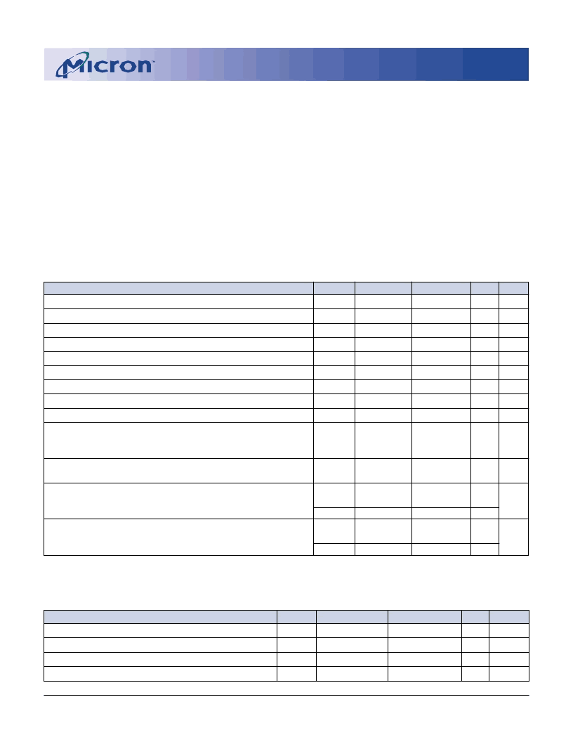
ABSOLUTE MAXIMUM RATINGS*
Voltage on V
DD
Supply
Relative to V
SS
............................................-1V to +3.6V
Voltage on V
DD
Q Supply
Relative to V
SS
............................................-1V to +3.6V
Voltage on V
REF
and Inputs
Relative to V
SS
............................................-1V to +3.6V
Voltage on I/O Pins
Relative to V
SS
...............................-0.5V to V
DD
Q +0.5V
Operating Temperature, T
A
(ambient) ...0°C to +70°C
Storage Temperature (plastic) ............-55°C to +150°C
Power Dissipation ........................................................ 2W
Short Circuit Output Current................................. 50mA
*Stresses greater than those listed under “Absolute
Maximum Ratings” may cause permanent damage to
the device. This is a stress rating only, and functional
operation of the device at these or any other conditions
above those indicated in the operational sections of
this specification is not implied. Exposure to absolute
maximum rating conditions for extended periods may
affect reliability.
AC INPUT OPERATING CONDITIONS
(Notes: 1-5, 14, 16, 40; notes appear on pages 46-49) (0°C
≤
T
A
≤
+70°C; V
DD
= +2.5V ±0.125V, V
DD
Q = +2.5V ±0.125V)
PARAMETER/CONDITION
Input High (Logic 1) Voltage; DQ
Input Low (Logic 0) Voltage; DQ
Clock Input Differential Voltage; CK and CK#
Clock Input Crossing Point Voltage; CK and CK#
SYMBOL
V
IH
(
AC
)
V
IL
(
AC
)
V
ID
(
AC
)
V
IX
(
AC
)
MIN
MAX
–
UNITS
V
V
V
V
NOTES
14, 28, 39
14, 28, 39
8
9
V
REF
+ 0.310
–
0.7
0.5xV
DD
Q-0.2
V
REF
- 0.310
V
DD
Q + 0.6
0.5xV
DD
Q+0.2
DC ELECTRICAL CHARACTERISTICS AND OPERATING CONDITIONS
(Notes: 1-5, 16, 40; notes appear on pages 46-49) (0°C
≤
T
A
≤
+70°C; V
DD
= +2.5V ±0.125V, V
DD
Q = +2.5V ±0.125V)
PARAMETER/CONDITION
Supply Voltage
I/O Supply Voltage
I/O Reference Voltage
I/O Termination Voltage (system)
Input High (Logic 1) Voltage
Input Low (Logic 0) Voltage
Clock Input Voltage Level; CK and CK#
Clock Input Differential Voltage; CK and CK#
Clock Input Crossing Point Voltage; CK and CK#
INPUT LEAKAGE CURRENT
Any input 0V
≤
V
IN
≤
V
DD
(All other pins not under test = 0V)
OUTPUT LEAKAGE CURRENT
(DQs are disabled; 0V
≤
V
OUT
≤
V
DD
Q)
OUTPUT LEVELS: Impedance Match
High Current (V
OUT
= V
DD
Q-0.373V, minimum V
REF
, minimum V
TT
)
Low Current (V
OUT
= 0.373V, maximum V
REF
,maximum V
TT
)
OUTPUT LEVELS: Reduced drive option -
High Current (V
OUT
= V
DD
Q-0.763V, minimum V
REF
, minimum V
TT
)
Low Current (V
OUT
= 0.763V, maximum V
REF
,maximum V
TT
)
SYMBOL
V
DD
V
DD
Q
V
REF
V
TT
V
IH
(
DC
)
V
IL
(
DC
)
V
IN
V
ID
V
IX
MIN
2.375
2.375
MAX
2.625
2.625
UNITS NOTES
V
V
V
V
V
V
V
V
V
40
6
7
28
28
0.49
x
V
DD
Q
V
REF
- 0.04
V
REF
+ 0.15
-0.3
-0.3
0.36
1.15
0.51
x
V
DD
Q
V
REF
+ 0.04
V
DD
+ 0.3
V
REF
- 0.15
V
DD
Q + 0.3
V
DD
Q + 0.6
1.35
8
9
I
I
-2
2
μA
I
OZ
-5
5
μA
I
OH
I
OL
-4
4
–
–
mA
mA
37, 39
I
OHR
I
OLR
-9
9
–
–
mA
mA
38, 39
相關(guān)PDF資料 |
PDF描述 |
|---|---|
| MT46V4M32LG | I.MX31 LITE KIT |
| MT46V64M4 | 16 Meg x 4 x 4 banks DDR SDRAM(16M x 4 x 4組,雙數(shù)據(jù)速率同步動(dòng)態(tài)RAM) |
| MT46V64M8 | 16 Meg x 8 x 4 banks DDR SDRAM(16M x 8 x 4組,雙數(shù)據(jù)速率同步動(dòng)態(tài)RAM) |
| MT48LC16M8A1TG | SYNCHRONOUS DRAM |
| MT48LC32M4A1 | ECONOLINE: RSZ/P - 1kVDC |
相關(guān)代理商/技術(shù)參數(shù) |
參數(shù)描述 |
|---|---|
| MT46V4M32LG | 制造商:MICRON 制造商全稱(chēng):Micron Technology 功能描述:DOUBLE DATA RATE DDR SDRAM |
| MT46V64M16 | 制造商:MICRON 制造商全稱(chēng):Micron Technology 功能描述:DOUBLE DATA RATE (DDR) SDRAM |
發(fā)布緊急采購(gòu),3分鐘左右您將得到回復(fù)。