- 您現(xiàn)在的位置:買賣IC網(wǎng) > PDF目錄378045 > PCI1221GHK (Texas Instruments, Inc.) KPT 11C 11#16 SKT PLUG PDF資料下載
參數(shù)資料
| 型號: | PCI1221GHK |
| 廠商: | Texas Instruments, Inc. |
| 英文描述: | KPT 11C 11#16 SKT PLUG |
| 中文描述: | PC卡控制器 |
| 文件頁數(shù): | 110/123頁 |
| 文件大小: | 1659K |
| 代理商: | PCI1221GHK |
第1頁第2頁第3頁第4頁第5頁第6頁第7頁第8頁第9頁第10頁第11頁第12頁第13頁第14頁第15頁第16頁第17頁第18頁第19頁第20頁第21頁第22頁第23頁第24頁第25頁第26頁第27頁第28頁第29頁第30頁第31頁第32頁第33頁第34頁第35頁第36頁第37頁第38頁第39頁第40頁第41頁第42頁第43頁第44頁第45頁第46頁第47頁第48頁第49頁第50頁第51頁第52頁第53頁第54頁第55頁第56頁第57頁第58頁第59頁第60頁第61頁第62頁第63頁第64頁第65頁第66頁第67頁第68頁第69頁第70頁第71頁第72頁第73頁第74頁第75頁第76頁第77頁第78頁第79頁第80頁第81頁第82頁第83頁第84頁第85頁第86頁第87頁第88頁第89頁第90頁第91頁第92頁第93頁第94頁第95頁第96頁第97頁第98頁第99頁第100頁第101頁第102頁第103頁第104頁第105頁第106頁第107頁第108頁第109頁當前第110頁第111頁第112頁第113頁第114頁第115頁第116頁第117頁第118頁第119頁第120頁第121頁第122頁第123頁
110
POST OFFICE BOX 655303
DALLAS, TEXAS 75265
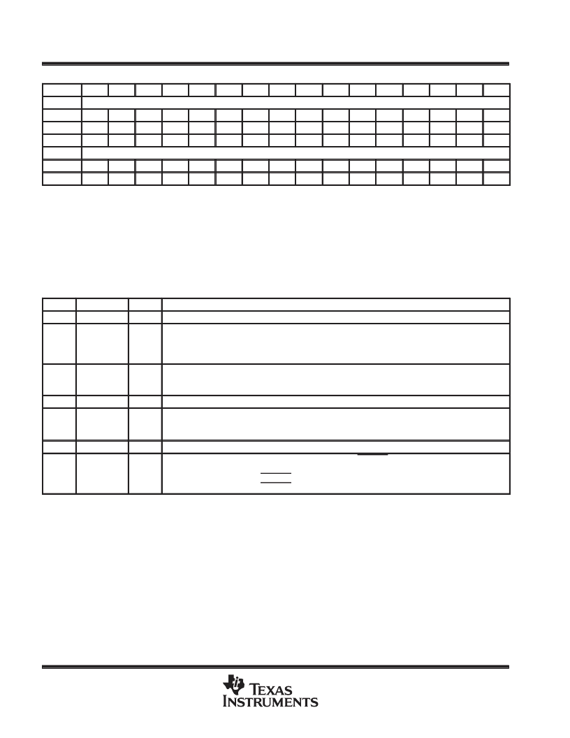
socket power management register
Bit
31
30
29
28
27
26
25
24
23
22
21
20
19
18
17
16
Name
Socket power management
Type
R
R
R
R
R
R
R
R
R
R
R
R
R
R
R
R/W
Default
0
0
0
0
0
0
0
0
0
0
0
0
0
0
0
0
Bit
15
14
13
12
11
10
9
8
7
6
5
4
3
2
1
0
Name
Socket power management
Type
R
R
R
R
R
R
R
R
R
R
R
R
R
R
R
R/W
Default
0
0
0
0
0
0
0
0
0
0
0
0
0
0
0
0
Register:
Type:
Offset:
Default:
Description: This register provides power management control over the socket through a mechanism for
slowing or stopping the clock on the card interface when the card is idle. See Table 58 for a
complete description of the register contents.
Socket power management
Read only, read/write (see individual bit descriptions)
CardBus socket address + 20h
0000 0000h
Table 58. Socket Power Management Register
BIT
SIGNAL
TYPE
FUNCTION
31-26
RSVD
R
Reserved. Bits 31-26 are read only and return 0s when read.
25
SKTACCES
R
Socket access status. This bit provides information on when a socket access has occurred. This bit is
cleared by a read access.
0 = A PC card access has not occurred (default).
1 = A PC card access has occurred.
24
SKTMODE
R
Socket mode status. This bit provides clock mode information.
0 = Clock is operating normally.
1 = Clock frequency has changed.
23-17
RSVD
R
Reserved. Bits 23-17 are read only and return 0s when read.
16
CLKCTRLEN
R/W
CardBus clock control enable. When bit 16 is set, clock control (CLKCTRL bit 0) is enabled.
0 = Clock control is disabled (default).
1 = Clock control is enabled.
15-1
RSVD
R
Reserved. Bits 15-1 are read only and return 0s when read.
0
CLKCTRL
R/W
CardBus clock control. This bit determines whether the CB CLKRUN protocol will attempt to stop or slow
the CB clock during idle states. Bit 16 enables this bit.
0 = Allows CB CLKRUN protocol to stop the CB clock (default).
1 = Allows CB CLKRUN protocol to slow the CB clock by a factor of 16.
相關PDF資料 |
PDF描述 |
|---|---|
| PCI1410GHK | PC CARD CONTROLLERS |
| PCI1510GVF | PC CARD CONTROLLERS |
| PCI1510ZVF | PC CARD CONTROLLERS |
| PCI1520I | PC CARD CONTROLLERS |
| PCI4410A | PC CARD AND OHCI CONTROLLER |
相關代理商/技術參數(shù) |
參數(shù)描述 |
|---|---|
| PCI1221PDV | 制造商:Rochester Electronics LLC 功能描述:- Bulk |
| PCI1225 | 制造商:TI 制造商全稱:Texas Instruments 功能描述:PC CARD CONTROLLERS |
| PCI1225GHK | 制造商:Texas Instruments 功能描述: |
| PCI1225PDV | 制造商:Rochester Electronics LLC 功能描述:- Bulk 制造商:Texas Instruments 功能描述: |
| PCI-1240U | 制造商:ADVANTECH 制造商全稱:Advantech Co., Ltd. 功能描述:4-axis Stepping and Servo Motor Control Universal PCI Card |
發(fā)布緊急采購,3分鐘左右您將得到回復。