- 您現在的位置:買賣IC網 > PDF目錄369953 > PCT789T-A PCI HSP56 World MicroModem/PCT303DW/PCT1789W PDF資料下載
參數資料
| 型號: | PCT789T-A |
| 英文描述: | PCI HSP56 World MicroModem/PCT303DW/PCT1789W |
| 中文描述: | 世界MicroModem/PCT303DW/PCT1789W的PCI HSP56 |
| 文件頁數: | 20/70頁 |
| 文件大小: | 872K |
| 代理商: | PCT789T-A |
第1頁第2頁第3頁第4頁第5頁第6頁第7頁第8頁第9頁第10頁第11頁第12頁第13頁第14頁第15頁第16頁第17頁第18頁第19頁當前第20頁第21頁第22頁第23頁第24頁第25頁第26頁第27頁第28頁第29頁第30頁第31頁第32頁第33頁第34頁第35頁第36頁第37頁第38頁第39頁第40頁第41頁第42頁第43頁第44頁第45頁第46頁第47頁第48頁第49頁第50頁第51頁第52頁第53頁第54頁第55頁第56頁第57頁第58頁第59頁第60頁第61頁第62頁第63頁第64頁第65頁第66頁第67頁第68頁第69頁第70頁

PC-TEL, Inc.
20
1789W0DOCDAT06A-0299
PCT1789W DATA SHEET
PCT303DW F
UNCTIONAL
D
ESCRIPTION
!
PRELIMINARY
PRELIMINARY
The digital interface consists of a single, synchronous
serial link which communicates both telephony and
control data.
In Serial mode 0 or 1, the PCT303D operates as a
master, where the master clock (MCLK) is an input, the
serial data clock (SCLK) is an output, and the frame
sync signal (FSYNC) is an output. The MCLK frequency
and the value of the sample rate control registers 7, 8, 9
and 10 determine the sample rate (Fs). The serial port
clock, SCLK, runs at 256 bits per frame, where the frame
rate is equivalent to the sample rate. Refer to “Clock
Generation Subsystem” on page 23 for more details on
programming sample rates.
The PCT303DW transfers 16-bit or 15-bit telephony
data in the primary timeslot and 16-bit control data in the
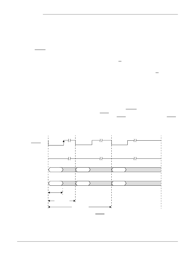
secondary timeslot. Figure 11 and Figure 12 show the
relative timing of the serial frames. Primary frames occur
at the frame rate and are always present. To minimize
overhead in the external DSP, secondary frames are
present only when requested.
Two methods exist for transferring control information in
the secondary frame. The default power-up mode uses
the LSB of the 16-bit transmit (TX) data word as a flag to
request a secondary transfer. In this mode, only 15-bit
TX data is transferred, resulting in a loss of SNR but
allowing software control of the secondary frames. As
an alternative method, the FC pin can serve as a
hardware flag for requesting a secondary frame. The
external DSP can turn on the 16-bit TX mode by setting
the SB bit of register 1. In the 16-bit TX mode, the
hardware FC pin must be used to request secondary
transfers.
Figure 13 and Figure 14 illustrate the secondary frame
read cycle and write cycle, respectively. During a read
cycle, the R/W bit is high and the 5-bit address field
contains the address of the register to be read. The
contents of the 8-bit control register are placed on the
SDO signal. During a write cycle, the R/W bit is low and
the 5-bit address field contains the address of the
register to be written. The 8-bit data to be written
immediately follows the address on SDI. Only one
register can be read or written during each secondary
frame. See “PCT303DW Control Registers” on page 41
for the register addresses and functions.
In serial mode 2, the PCT303D operates as a slave
device, where the MCLK is an input, the SCLK is a no
connect, and the FSYNC is an input. In addition, the
RGDT/FSD pin operates as a delayed frame sync (FSD)
and the FC/RGDT pin operates as ring detect (RGDT).
Note that in this mode, FC operation is not supported.
XMT Data
Secondary
Update
FSYNC
Primary
Secondary
Primary
Communications Frame 1 (CF1)
(CF2)
FC
0
Secondary
Update
XMT Data
RCV Data
D15-D1 D0=1 (Software FC Bit)
128 SCLKs
256 SCLKs
16 SCLKS
SDI
SDO
RCV Data
Figure 11 Software FC/RGDT Secondary Request
相關PDF資料 |
PDF描述 |
|---|---|
| PCX-150 | 150A QUASI- CW LASER DIODE DRIVER/PULSED CURRENT SOURCE |
| PCX-6220 | 150A 40V QUASI-CW LASER DIODE DRIVER/PULSED CURRENT SOURCE |
| PCXO116 | Logic IC |
| PD-110A | CAP,CERM,TRIM,5mm,9-50pf, 200VDC COLOR GREEN,2 LEADS |
| PD-110B | CAP,CERM,TRIM,8mm,8.5-100pF, 250V,COLOR PURPLE |
相關代理商/技術參數 |
參數描述 |
|---|---|
| PCT789T-C | 制造商:PCTEL 功能描述:PCI MODEM CHIP |
| PCT789T-C1 | 制造商:Rochester Electronics LLC 功能描述:- Bulk |
| PCT900 | 制造商:General Tools 功能描述:Combination Contact/Non-Contact Laser Tachometer 制造商:General Tools 功能描述:TACHOMETERMINI PHOTO |
| PCT-A | 制造商:Cooper Interconnect 功能描述: 制造商:Cooper Bussmann 功能描述: 制造商:COOPER BUSSMANN 功能描述:Fuse Holder 125V Pin Through Hole |
| PCTABLE | 制造商:Black Box Corporation 功能描述:PC / UTILITY TABLE 28"H X 36"W X 24"D |
發(fā)布緊急采購,3分鐘左右您將得到回復。