- 您現(xiàn)在的位置:買賣IC網(wǎng) > PDF目錄367908 > pentium II (Intel Corp.) pentium II processor With On-die Cache Mobile Module Connector 1 (MMC-1)(帶緩存和連接器1的奔II處理器) PDF資料下載
參數(shù)資料
| 型號: | pentium II |
| 廠商: | Intel Corp. |
| 英文描述: | pentium II processor With On-die Cache Mobile Module Connector 1 (MMC-1)(帶緩存和連接器1的奔II處理器) |
| 中文描述: | 奔騰II處理器芯片上緩存手機(jī)模塊連接器1(MMC管理- 1)(帶緩存和連接器1的奔二處理器) |
| 文件頁數(shù): | 14/34頁 |
| 文件大?。?/td> | 582K |
| 代理商: | PENTIUM II |
第1頁第2頁第3頁第4頁第5頁第6頁第7頁第8頁第9頁第10頁第11頁第12頁第13頁當(dāng)前第14頁第15頁第16頁第17頁第18頁第19頁第20頁第21頁第22頁第23頁第24頁第25頁第26頁第27頁第28頁第29頁第30頁第31頁第32頁第33頁第34頁
14
Intel
a
Pentium
a
II Processor With On-die Cache Mobile Module MMC-1
3.1.7
Voltages (39 Signals)
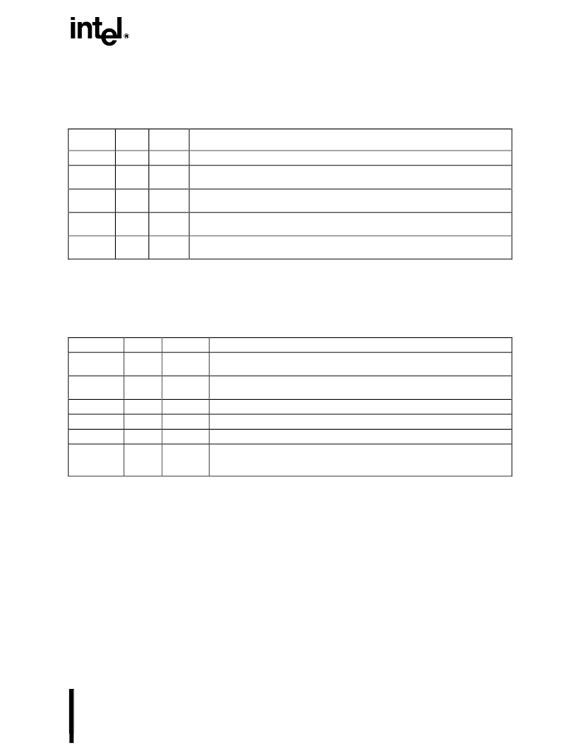
Table 7 lists the voltage signal definitions.
Table 7. Voltage Descriptions
Name
Type
Number
of Pins
Description
V_DC
I
10
DC Input:
5V-21V.
V_3S
I
20
SUSB# controlled 3.3V:
V_3S is supplied by the system electronics. This is a 3.3V power
supply that is turned off during suspend during system states STR, STD, and Soff.
V_5
I
1
SUSC# controlled 5V:
Power managed 5.0-V supply.
An output of the voltage regulator on
the system electronics. This rail is off during STD and Soff.
V_3
I
5
SUSC# controlled 3.3V:
Power managed 3.3-V supply.
An output of the voltage regulator on
the system electronics. This rail is off during STD and Soff.
V_CPUIO
O
3
Processor I/O Ring:
Powers the processor interface signals such as the PIIX4E/M open-drain
pullups for the processor/PIIX4E/M sideband signals and the CKDM66-M clock source.
3.1.8
JTAG (7 Signals)
Table 8 lists the JTAG signals, which the system electronics
can use to implement a JTAG chain and ITP port, if desired.
The JTAG signals provided cannot be used as an ITP port,
since the definition of the ITP interface has changed
between the generations of the mobile Pentium processor
and the mobile Pentium II processor with on-die cache.
Table 8. JTAG Pins
Name
Type
Voltage
Description
TDO
O
V_CPUIO
JTAG Test Data Out:
Serial output port. TAP instructions and data is shifted out of the
processor from this port.
TDI
I
V_CPUIO
JTAG Test Data In:
Serial input port. TAP instructions and data is shifted into the
processor from this port.
TMS
I
V_CPUIO
JTAG Test Mode Select:
Controls the TAP controller change sequence.
TCLK
I
V_CPUIO
JTAG Test Clock:
Testability clock for clocking the JTAG boundary scan sequence.
TRST#
I
V_CPUIO
JTAG Test Reset:
Asynchronously resets the TAP controller in the processor.
ITP(1:0)
ITP1
ITP0
O
I
V_CPUIO
Debug Port Signals:
These signals are not used on the module and should not be
connected.
NOTE:
DBREST# (reset target system) on the ITP debug port can be “l(fā)ogically ANDed” with VR_PWRGD TO PIIX4E/M’s PWROK.
相關(guān)PDF資料 |
PDF描述 |
|---|---|
| PERICOMPI7C8150 | 2-Port PCI-to-PCI Bridge |
| PESDXL2BT | Low capacitance double bidirectional ESD protection diodes in SOT23 |
| PESDXL2UM | LJT 23C 21#20 2#16 PIN RECP |
| PETAM1270BK300R | BRAID SLEEVING 300M |
| PETAM1270BK50C | 5V RS232 Transceiver with One Receiver Active in SHUTDOWN |
相關(guān)代理商/技術(shù)參數(shù) |
參數(shù)描述 |
|---|---|
| P-ENV568K3G3 | 制造商:Panasonic Industrial Company 功能描述:TUNER |
| PEO14012 | 制造商:TE Connectivity 功能描述:RELAY SPCO 12VDC |
| PEO14024 | 制造商:TE Connectivity 功能描述:RELAY SPCO 24VDC |
| PEO96742 | 制造商:Delphi Corporation 功能描述:ASM TERM |
| PEOODO3A | 制造商:MACOM 制造商全稱:Tyco Electronics 功能描述:Versatile Power Entry Module with Small Footprint |
發(fā)布緊急采購,3分鐘左右您將得到回復(fù)。