- 您現(xiàn)在的位置:買(mǎi)賣(mài)IC網(wǎng) > PDF目錄361304 > QR0001 PDF資料下載
參數(shù)資料
| 型號(hào): | QR0001 |
| 文件頁(yè)數(shù): | 28/40頁(yè) |
| 文件大?。?/td> | 440K |
| 代理商: | QR0001 |
第1頁(yè)第2頁(yè)第3頁(yè)第4頁(yè)第5頁(yè)第6頁(yè)第7頁(yè)第8頁(yè)第9頁(yè)第10頁(yè)第11頁(yè)第12頁(yè)第13頁(yè)第14頁(yè)第15頁(yè)第16頁(yè)第17頁(yè)第18頁(yè)第19頁(yè)第20頁(yè)第21頁(yè)第22頁(yè)第23頁(yè)第24頁(yè)第25頁(yè)第26頁(yè)第27頁(yè)當(dāng)前第28頁(yè)第29頁(yè)第30頁(yè)第31頁(yè)第32頁(yè)第33頁(yè)第34頁(yè)第35頁(yè)第36頁(yè)第37頁(yè)第38頁(yè)第39頁(yè)第40頁(yè)

11.0 Board Considerations
(Continued)
2.86 ns. The QuickRing UpPort needs 2.36 ns of this bit
width (including transitions) to successfully sample the val-
ue for each sub-symbol. This allows for a total skew budget
of 0.5 ns. The interconnect between DnPort and UpPort
should be limited to 350 ps. This provides 150 ps skew mar-
gin. The 350 ps can be divided between PCB traces, con-
nectors, headers, cables and all other media used in the
signal path.
The skew within a pair needs to be controlled because of
the EMI considerations. The simultaneous and opposite
transitions on paths within a pair create equal and opposing
electromagnetic fields. These EMF, the source of EMI,
serve to cancel each other thereby reducing EMI. The skew
within a pair should be controlled so that the single ended
EMF remain temporally and spatially relevant for the cancel-
ing affect.
The length of node interconnects is not critical to the opera-
tion of QuickRing until it degrades signal integrity. Nodes in
a ring can have different length interconnects. The maxi-
mum length of the interconnect depends on two qualities of
the interconnect; transition time degradation and amplitude
antenuation. Any extension in transition time due to the high
frequency filter affect of the interconnect, takes away from
the skew budget. The trade offs between the skew and tran-
sition time degradation must be balanced to allow for the
correct amount of sample time for the UpPort.
The signal attenuation affects the differential signal ampli-
tude at the receiver input. The receiver requires a differen-
tial voltage of at least 100 mV to guarantee a state. The
receiver actually is more sensitive than that under typical
operating conditions, but due to power supply and tempera-
ture variations, and test limitations, this is the data sheet
specification. As long as the differential voltage is guaran-
teed to be at least 150 mV and all the skew budget specifi-
cations are met, the receiver will operate correctly with ade-
quate noise margin.
12.0 Power and Decoupling Issues
12.1 Power Issues
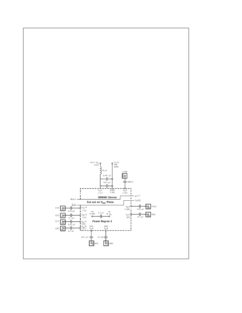
The QR0001 device internally has Four distinct Power re-
gions. These regions are labeled (Refer to Figure 12.3):
1. Logic Power Pins
(V
CC
4,5,12,13; GND 3,15,18,19,28,29);
2. Client Receive Port Output Power Pins
(V
CC
6,7,8,9,10,11; GND 20,21,22,23,24,25,26,27);
3. LVDS Power Pins
(V
CC
1,3; GND 1,2,4,5,6,7,8,10,11,12,13,14,16,17);
4. PLL and Delay Element Power Pins
(V
CC
2; GND 9);.
It is currently recommended that the PC Board have sepa-
rate GND and V
CC
planes. Also, Power Region 2 should
have some additional isolation from the power plane. Com-
plete isolation is not required. The isolation aids in limiting
the Receive Port current spikes to the remaining plane. Re-
fer to Figure 12.1.
12.2 Decoupling Issues
lt is currently recommended that capacitors be placed local-
ly on all four corners of the device to provide an even filter-
ing. Capacitors should also be placed close to power region
2 to provide additional noise filtering. Refer to Figure 12.1.
Two capacitors should be placed in parallel to get high and
low frequency filtering along each side. However, each ca-
pacitor should have a via directiy to the V
CC
and Ground
planes.
For power region 4 (PLL and Delay Element Power Pin), two
decoupling capacitors should be placed as close to the pins
as possible (between V
CC2
and GND9). A trace from the pin
directly to the capacitors is recommended and separate
vias to ground plane for each capacitor. Refer to Figure
12.1.
TL/F/11928–28
FIGURE 12.1. QR0001 Power Region Isolation
28
相關(guān)PDF資料 |
PDF描述 |
|---|---|
| QR0610T30 | 128 x 128 pixel format, LED Backlight available |
| QRD0610T30 | 128 x 128 pixel format, LED or EL Backlight available |
| QRC0610T30 | 128 x 128 pixel format, LED or EL Backlight available |
| QRF0610T30 | 128 x 128 pixel format, LED or EL Backlight available |
| QR0620T30 | 128 x 128 pixel format, LED or EL Backlight available |
相關(guān)代理商/技術(shù)參數(shù) |
參數(shù)描述 |
|---|---|
| QR0610T30 | 制造商:POWEREX 制造商全稱(chēng):Powerex Power Semiconductors 功能描述:Fast Recovery Diode Module (100 Amp/600 Volts) |
| QR0620T30 | 制造商:POWEREX 制造商全稱(chēng):Powerex Power Semiconductors 功能描述:Fast Recovery Diode Module (200 Amp/600 Volts) |
| QR0630T30 | 制造商:POWEREX 制造商全稱(chēng):Powerex Power Semiconductors 功能描述:Fast Recovery Diode Module (300 Amp/600 Volts) |
| QR0640T30 | 制造商:POWEREX 制造商全稱(chēng):Powerex Power Semiconductors 功能描述:Fast Recovery Diode Module (400 Amp/600 Volts) |
| QR06A-2/106349 | 功能描述:BLWR CROSS FLOW 460X158MM 115VAC RoHS:是 類(lèi)別:風(fēng)扇,熱管理 >> 風(fēng)扇 - AC 系列:QR06 其它有關(guān)文件:Declaration of Conformity 標(biāo)準(zhǔn)包裝:1 系列:- 氣流:- 軸承類(lèi)型:- 風(fēng)扇類(lèi)型:- 特點(diǎn):- 雜訊:- 功率(瓦特):- RPM:- 尺寸/尺寸:- 靜態(tài)壓力:- 端子:- 電壓 - 額定:- 重量:- 額定電流:- 預(yù)期壽命:- 工作溫度:- 電壓范圍:- 其它名稱(chēng):Q5464961 |
發(fā)布緊急采購(gòu),3分鐘左右您將得到回復(fù)。