- 您現(xiàn)在的位置:買賣IC網(wǎng) > PDF目錄373275 > RK80530KZ017512 MICROPROCESSOR|32-BIT|CMOS|PGA|370PIN|CERAMIC PDF資料下載
參數(shù)資料
| 型號: | RK80530KZ017512 |
| 英文描述: | MICROPROCESSOR|32-BIT|CMOS|PGA|370PIN|CERAMIC |
| 中文描述: | 微處理器| 32位|的CMOS |美巡賽| 370PIN |陶瓷 |
| 文件頁數(shù): | 76/86頁 |
| 文件大?。?/td> | 882K |
| 代理商: | RK80530KZ017512 |
第1頁第2頁第3頁第4頁第5頁第6頁第7頁第8頁第9頁第10頁第11頁第12頁第13頁第14頁第15頁第16頁第17頁第18頁第19頁第20頁第21頁第22頁第23頁第24頁第25頁第26頁第27頁第28頁第29頁第30頁第31頁第32頁第33頁第34頁第35頁第36頁第37頁第38頁第39頁第40頁第41頁第42頁第43頁第44頁第45頁第46頁第47頁第48頁第49頁第50頁第51頁第52頁第53頁第54頁第55頁第56頁第57頁第58頁第59頁第60頁第61頁第62頁第63頁第64頁第65頁第66頁第67頁第68頁第69頁第70頁第71頁第72頁第73頁第74頁第75頁當(dāng)前第76頁第77頁第78頁第79頁第80頁第81頁第82頁第83頁第84頁第85頁第86頁
76
Datasheet
Intel
Pentium
III Processor with 512KB L2 Cache at 1.13GHz to 1.40GHz
7.0
Processor Signal Description
This section provides an alphabetical listing of all the Intel Pentium
III
processor with 512 KB
L2 Cache signals. The tables at the end of this section summarize the signals by direction: output,
input, and I/O.
7.1
Alphabetical Signals Reference
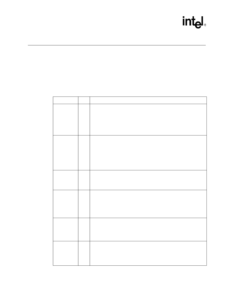
Table 39. Signal Description (Sheet 1 of 9)
Name
Type
Description
A20M#
I
If the A20M# (Address-20 Mask) input signal is asserted, the processor masks
physical address bit 20 (A20#) before looking up a line in any internal cache and
before driving a read/write transaction on the bus. Asserting A20M# emulates the
8086 processor's address wrap-around at the 1MB boundary. Assertion of A20M#
is only supported in real mode.
A20M# is an asynchronous signal. However, to ensure recognition of this signal
following an I/O write instruction, it must be valid along with the TRDY# assertion of
the corresponding I/O Write bus transaction.
A[35:3]#
I/O
The A[35:3]# (Address) signals define a 2
36
-byte physical memory address space.
When ADS# is active, these pins transmit the address of a transaction; when ADS#
is inactive, these pins transmit transaction type information. These signals must
connect the appropriate pins of all agents on the processor system bus. The
A[35:24]# signals are parity-protected by the AP1# parity signal, and the A[23:3]#
signals are parity-protected by the AP0# parity signal.
On the active-to-inactive transition of RESET#, the processors sample the A[35:3]#
pins to determine their power-on configuration. See the Intel
Pentium
II
Processor Developer’s Manual
for details.
ADS#
I/O
The ADS# (Address Strobe) signal is asserted to indicate the validity of the
transaction address on the A[35:3]# pins. All bus agents observe the ADS#
activation to begin parity checking, protocol checking, address decode, internal
snoop, or deferred reply ID match operations associated with the new transaction.
This signal must connect the appropriate pins on all processor system bus agents.
AERR#
I/O
The AERR# (Address Parity Error) signal is observed and driven by all processor
system bus agents, and if used, must connect the appropriate pins on all processor
system bus agents. AERR# observation is optionally enabled during power-on
configuration; if enabled, a valid assertion of AERR# aborts the current transaction.
If AERR# observation is disabled during power-on configuration, a central agent
may handle an assertion of AERR# as appropriate to the error handling architecture
of the system.
AP[1:0]#
I/O
The AP[1:0]# (Address Parity) signals are driven by the request initiator along with
ADS#, A[35:3]#, REQ[4:0]#, and RP#. AP1# covers A[35:24]#, and AP0# covers
A[23:3]#. A correct parity signal is high if an even number of covered signals are
low and low if an odd number of covered signals are low. This allows parity to be
high when all the covered signals are high. AP[1:0]# should connect the appropriate
pins of all processor system bus agents.
BCLK/BCLK#
I
The BCLK (Bus Clock) and BCLK# (for differential clock) signals determines the
bus frequency. All processor system bus agents must receive this signal to drive
their outputs and latch their inputs on the rising edge of BCLK. For differential
clocking, all processor system bus agents must receive this signal to drive their
outputs and latch their inputs on the BCLK and BCLK# crossing point.
All external timing parameters are specified with respect to the BCLK signal.
相關(guān)PDF資料 |
PDF描述 |
|---|---|
| RK80532PC041512 | Microprocessor |
| RK9410 | TRANSISTOR | MOSFET | N-CHANNEL | 30V V(BR)DSS | 7A I(D) | SO |
| RKC-SERIES | Interface IC |
| RKCB-SERIES | Interface IC |
| RKCR-SERIES | Interface IC |
相關(guān)代理商/技術(shù)參數(shù) |
參數(shù)描述 |
|---|---|
| RK80530KZ017512S L5XL | 制造商:Intel 功能描述:32BIT MPU 80530KZ017512 1.40G |
| RK80530KZ017512S L6BY | 制造商:Intel 功能描述:MPU Pentium 制造商:Intel 功能描述:MPU Pentium? III Processor-S 64-Bit 0.13um 1.4GHz 370-Pin FCPGA2 |
| RK80530PZ001256 | 制造商:未知廠家 制造商全稱:未知廠家 功能描述:Microprocessor |
| RK80530PZ006256 | 制造商:未知廠家 制造商全稱:未知廠家 功能描述:Microprocessor |
| RK80530PZ009256 | 制造商:Rochester Electronics LLC 功能描述:PIII 1.2G 256 ON DIE CACHE FC-PGA2 - Bulk |
發(fā)布緊急采購,3分鐘左右您將得到回復(fù)。