- 您現(xiàn)在的位置:買賣IC網(wǎng) > PDF目錄373275 > RK80530KZ017512 MICROPROCESSOR|32-BIT|CMOS|PGA|370PIN|CERAMIC PDF資料下載
參數(shù)資料
| 型號(hào): | RK80530KZ017512 |
| 英文描述: | MICROPROCESSOR|32-BIT|CMOS|PGA|370PIN|CERAMIC |
| 中文描述: | 微處理器| 32位|的CMOS |美巡賽| 370PIN |陶瓷 |
| 文件頁數(shù): | 78/86頁 |
| 文件大小: | 882K |
| 代理商: | RK80530KZ017512 |
第1頁第2頁第3頁第4頁第5頁第6頁第7頁第8頁第9頁第10頁第11頁第12頁第13頁第14頁第15頁第16頁第17頁第18頁第19頁第20頁第21頁第22頁第23頁第24頁第25頁第26頁第27頁第28頁第29頁第30頁第31頁第32頁第33頁第34頁第35頁第36頁第37頁第38頁第39頁第40頁第41頁第42頁第43頁第44頁第45頁第46頁第47頁第48頁第49頁第50頁第51頁第52頁第53頁第54頁第55頁第56頁第57頁第58頁第59頁第60頁第61頁第62頁第63頁第64頁第65頁第66頁第67頁第68頁第69頁第70頁第71頁第72頁第73頁第74頁第75頁第76頁第77頁當(dāng)前第78頁第79頁第80頁第81頁第82頁第83頁第84頁第85頁第86頁
78
Datasheet
Intel
Pentium
III Processor with 512KB L2 Cache at 1.13GHz to 1.40GHz
BR0#/BR1#
I/O
The BR0# and BR1#(Bus Request) pins drive the BREQ[1:0]# signals in the
system. The BREQ[1:0]# signals are interconnected in a rotating manner to
individual processor pins. The table below gives the rotating interconnect between
the processor and bus signals.
During power-up configuration, the central agent asserts the BR0# bus signal in the
system to assign the symmetric agent ID to the processor. The processor samples
its BR0# pin on the active-to-inactive transition of the RESET# to obtain its
symmetric agent ID. The processor asserts the BR0# pin to request the system
bus. All agents then configure their pins to match the appropriate bus signal
protocol, as shown below.
For uni-processor designs, BR0# must be connected to a 10-56
resistor to V
.
Refer to the platform design guide for implementation detail and resistor tolerance.
BSEL[1:0]
O
The BSEL signals are CMOS signals which are used to select the system bus
frequency. A BSEL[1:0] = ‘11’ selects a 133 MHz system bus frequency. The
frequency is determined by the processor(s), chipset, and frequency synthesizer
capabilities. All system bus agents must operate at the same frequency. The Intel
Pentium III processor with 512KB L2 Cache operates at 133 MHz system bus
frequency.
These signals must be pulled up to 3.3V power rail with 330 - 1 K
resistors and
provided as a frequency selection signal to the clock driver/synthesizer and chipset.
Refer to the platform design guide for implementation detail and resistor tolerance.
CLKREF
I
In Single-ended clock mode the CLKREF input is a filtered 1.25V supply voltage for
the processor PLL. A voltage divider and decoupling solution is provided by the
motherboard. See the design guide for implementation details.
When the processor operates in differential clock mode, this signal becomes
BCLK#.
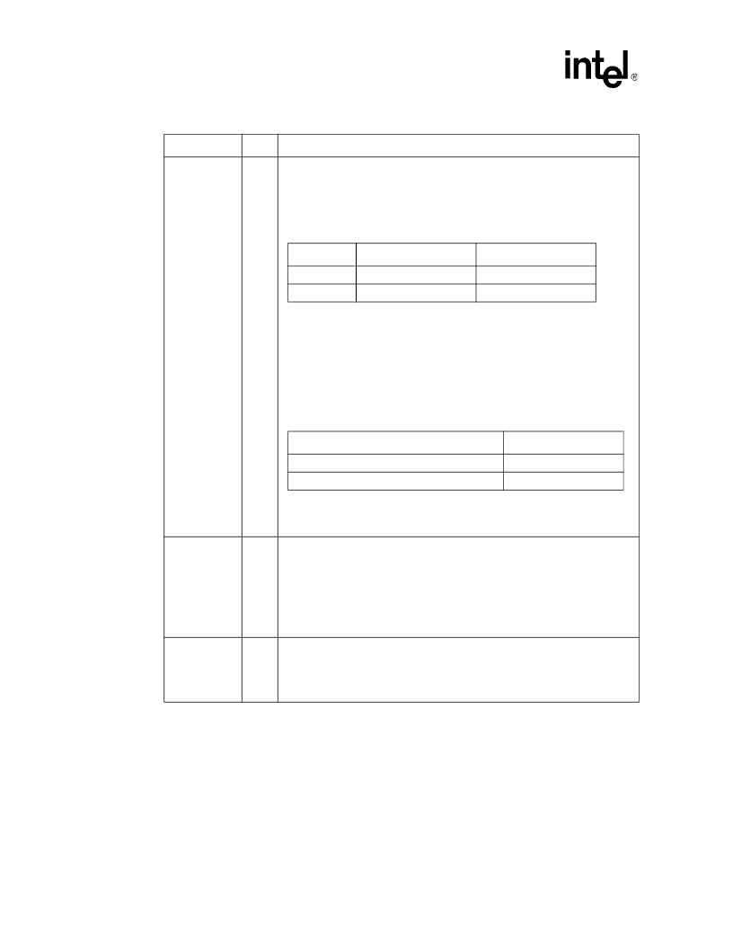
Table 39. Signal Description (Sheet 3 of 9)
Name
Type
Description
BR0# (I/O) and BR1# Signals Rotating Interconnect
Bus Signal
Agent 0 Pins
Agent 1 Pins
BREQ0#
BR0#
BR1#
BREQ1#
BR1#
BR0#
BR0# (I/O) and BR1# Signals Rotating Interconnect
Pin Sampled Active in RESET#
Agent ID
BR0#
0
BR1#
3
相關(guān)PDF資料 |
PDF描述 |
|---|---|
| RK80532PC041512 | Microprocessor |
| RK9410 | TRANSISTOR | MOSFET | N-CHANNEL | 30V V(BR)DSS | 7A I(D) | SO |
| RKC-SERIES | Interface IC |
| RKCB-SERIES | Interface IC |
| RKCR-SERIES | Interface IC |
相關(guān)代理商/技術(shù)參數(shù) |
參數(shù)描述 |
|---|---|
| RK80530KZ017512S L5XL | 制造商:Intel 功能描述:32BIT MPU 80530KZ017512 1.40G |
| RK80530KZ017512S L6BY | 制造商:Intel 功能描述:MPU Pentium 制造商:Intel 功能描述:MPU Pentium? III Processor-S 64-Bit 0.13um 1.4GHz 370-Pin FCPGA2 |
| RK80530PZ001256 | 制造商:未知廠家 制造商全稱:未知廠家 功能描述:Microprocessor |
| RK80530PZ006256 | 制造商:未知廠家 制造商全稱:未知廠家 功能描述:Microprocessor |
| RK80530PZ009256 | 制造商:Rochester Electronics LLC 功能描述:PIII 1.2G 256 ON DIE CACHE FC-PGA2 - Bulk |
發(fā)布緊急采購,3分鐘左右您將得到回復(fù)。