- 您現(xiàn)在的位置:買賣IC網(wǎng) > PDF目錄372283 > SST-MELODY-DAP SST-Melody®:-DAP: Audio Processor Data Sheet (Rev. 0. 10/02) PDF資料下載
參數(shù)資料
| 型號(hào): | SST-MELODY-DAP |
| 英文描述: | SST-Melody®:-DAP: Audio Processor Data Sheet (Rev. 0. 10/02) |
| 文件頁(yè)數(shù): | 8/24頁(yè) |
| 文件大?。?/td> | 585K |
| 代理商: | SST-MELODY-DAP |
第1頁(yè)第2頁(yè)第3頁(yè)第4頁(yè)第5頁(yè)第6頁(yè)第7頁(yè)當(dāng)前第8頁(yè)第9頁(yè)第10頁(yè)第11頁(yè)第12頁(yè)第13頁(yè)第14頁(yè)第15頁(yè)第16頁(yè)第17頁(yè)第18頁(yè)第19頁(yè)第20頁(yè)第21頁(yè)第22頁(yè)第23頁(yè)第24頁(yè)
REV. 0
–8–
SST-Melody-DAP
Assumptions:
External data memory is accessed every cycle with 50% of the
address pins switching.
External data memory writes occur every other cycle with
50% of the data pins switching.
Each address and data pin has a 10 pF total load at the pin.
The application operates at V
DDEXT
= 3.3 V and
t
CK
= 30 ns.
Total Power Dissipation
=
P
INT
+ (
C
V
DDEXT
2
f
)
P
INT
= internal power dissipation from Power vs. Frequency
graph (see Figures 2a through 2c).
(
C
V
DDEXT2
f
) is calculated for each output:
Table III. Power Dissipation Example
No. of
Pins
C
(pF) (V)
V
DDEXT2
f
(MHz)
(mW)
PD
Parameter
Address
Data Output,
WR
RD
CLKOUT,
DMS
Total
7
9
1
2
10
10
10
10
3.3
2
3.3
2
3.3
2
3.3
2
16.67
16.67
16.67
33.3
12.7
16.6
1.8
7.2
38.2
Total power dissipation for this example is P
INT
+ 38.0 mW.
Output Drive Currents
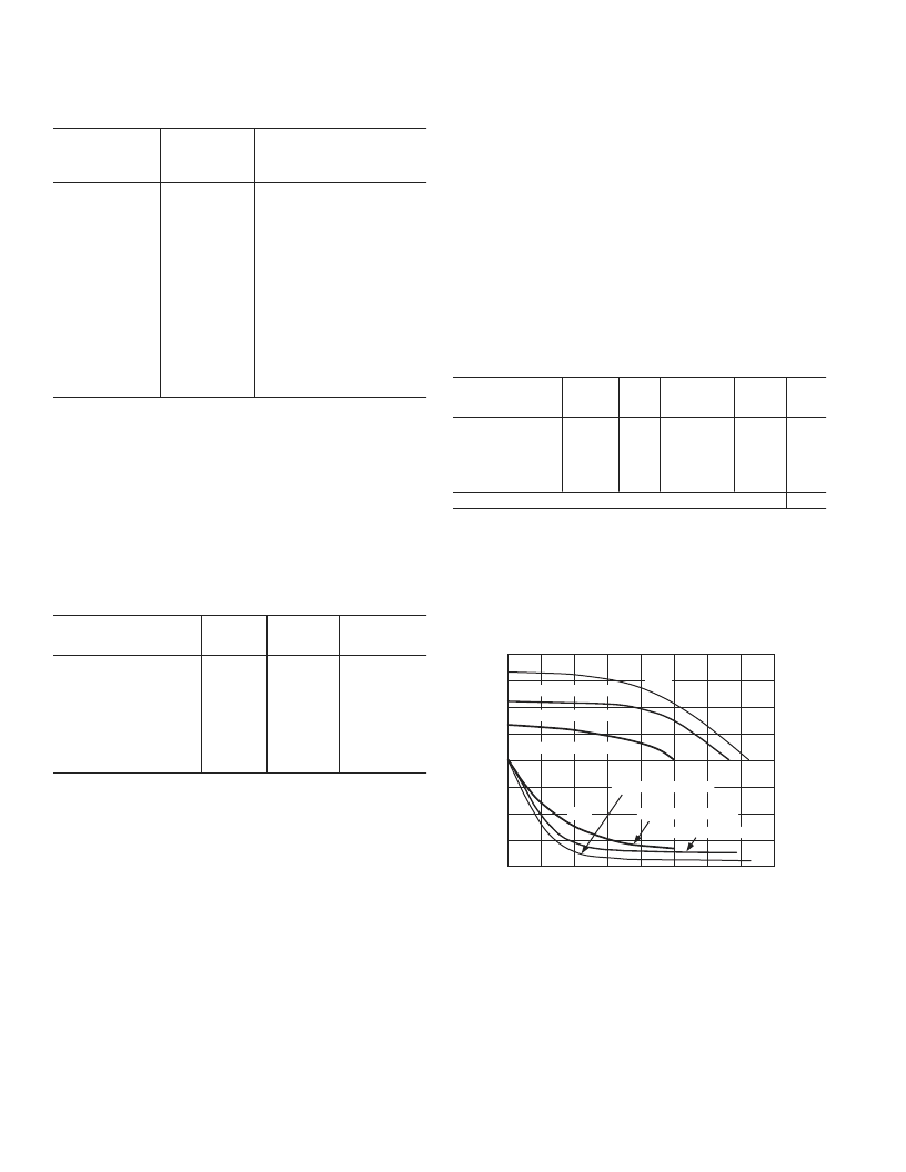
Figure 1 shows typical I–V characteristics for the output
drivers
on the SST-Melody-DAP. The curves represent the
current drive
capability of the output drivers as a function of
output voltage.
SOURCE VOLTAGE – V
–80
0
S
0.5
1.0
1.5
2.0
2.5
3.0
3.5
4.0
–60
–40
–20
0
20
40
60
80
V
DDEXT
– 3.6V @ –40 C
V
DDEXT
– 3.3V @ +25 C
V
DDEXT
– 2.5V @ +85 C
V
OH
V
OL
V
DDEXT
– 3.6V @ –40 C
V
DDEXT
– 2.5V @ +85 C
V
DDEXT
– 3.3V @ +25 C
Figure 1. Typical Output Driver Characteristics
Table I. Memory Timing Specifications
Memory
Device
Specification
Timing
Parameter
Definition
*
Parameter
Address Setup to
Write Start
Address Setup to
Write End
Address Hold
Time
Data Setup Time
Data Hold Time
OE to Data Valid
Address Access
Time
t
ASW
A0–A13,
xMS
Setup
before
WR
Low
A0–A13,
xMS
Setup
before
WR
Deasserted
A0–A13,
xMS
Hold
before
WR
Low
Data Setup before
WR
High
Data Hold after
WR
High
RD
Low to Data Valid
A0–A13,
xMS
to
Data Valid
t
AW
t
WRA
t
DW
t
DH
t
RDD
t
AA
*
xMS
=
PMS
,
DMS
,
CMS
, or
IOMS
.
FREQUENCY DEPENDENCY FOR TIMING
SPECIFICATIONS
t
CK
is defined as 0.5 t
CKI
. The SST-Melody-DAP uses an input
clock with a frequency equal to half the instruction rate. For
example, a 37.50 MHz input clock (which is equivalent to 26.6 ns)
yields a 13.3 ns processor cycle (equivalent to 75 MHz). t
CK
values within the range of 0.5 t
CKI
period should be substituted
for all relevant timing parameters to obtain the specification value.
Example: t
CKH
= 0.5 t
CK
– 2 ns = 0.5 (15 ns) – 2 ns = 5.5 ns
Table II. Environmental Conditions
*
Rating
Description
Symbol
LQFP
48
°
C/W
Mini-BGA
63.3
°
C/W
Thermal Resistance
(Case-to-Ambient)
Thermal Resistance
(Junction-to-Ambient)
Thermal Resistance
(Junction-to-Case)
CA
JA
50
°
C/W
70.7
°
C/W
JC
2
°
C/W
7.4
°
C/W
*
Where the Ambient Temperature Rating (T
AMB
) is:
T
AMB
= T
CASE
– (PD
CA
)
T
CASE
= Case Temperature in
°
C
PD = Power Dissipation in W
POWER DISSIPATION
To determine total power dissipation in a specific application,
the following equation should be applied for each output:
C V
f
DD
×
2
C
= load capacitance,
f
= output switching frequency.
Example:
In an application where external data memory is used and no
other outputs are active, power dissipation is calculated as follows:
相關(guān)PDF資料 |
PDF描述 |
|---|---|
| SST112-T1 | TRANSISTOR J-FET SOT-23 |
| SST113-T1 | TRANSISTOR J-FET SOT-23 |
| SST177-T1 | TRANSISTOR J-FET SOT-23 |
| SST1A1000B | Analog IC |
| SST1A800B | Analog IC |
相關(guān)代理商/技術(shù)參數(shù) |
參數(shù)描述 |
|---|---|
| SST-NAS-DN1 | 制造商:Molex 功能描述:DIAG, DEVICENET, NETALYTIX, S/W |
| SSTP600240D25 | 制造商:Teledyne Industrial 功能描述: |
| SSTPAD | 制造商:LINEAR 制造商全稱:LINEAR 功能描述:PICO AMPERE DIODES |
| SSTPAD1 | 制造商:LINEAR 制造商全稱:LINEAR 功能描述:PICO AMPERE DIODES |
| SSTPAD10 | 制造商:LINEAR 制造商全稱:LINEAR 功能描述:PICO AMPERE DIODES |
發(fā)布緊急采購(gòu),3分鐘左右您將得到回復(fù)。