- 您現(xiàn)在的位置:買(mǎi)賣(mài)IC網(wǎng) > PDF目錄385870 > ST63E69D1 (意法半導(dǎo)體) 8-BIT HCMOS MCU FOR DIGITAL CONTROLLED MULTI FREQUENCYMONITOR PDF資料下載
參數(shù)資料
| 型號(hào): | ST63E69D1 |
| 廠商: | 意法半導(dǎo)體 |
| 英文描述: | 8-BIT HCMOS MCU FOR DIGITAL CONTROLLED MULTI FREQUENCYMONITOR |
| 中文描述: | 8位HCMOS單片機(jī)的數(shù)控多FREQUENCYMONITOR |
| 文件頁(yè)數(shù): | 20/71頁(yè) |
| 文件大?。?/td> | 584K |
| 代理商: | ST63E69D1 |
第1頁(yè)第2頁(yè)第3頁(yè)第4頁(yè)第5頁(yè)第6頁(yè)第7頁(yè)第8頁(yè)第9頁(yè)第10頁(yè)第11頁(yè)第12頁(yè)第13頁(yè)第14頁(yè)第15頁(yè)第16頁(yè)第17頁(yè)第18頁(yè)第19頁(yè)當(dāng)前第20頁(yè)第21頁(yè)第22頁(yè)第23頁(yè)第24頁(yè)第25頁(yè)第26頁(yè)第27頁(yè)第28頁(yè)第29頁(yè)第30頁(yè)第31頁(yè)第32頁(yè)第33頁(yè)第34頁(yè)第35頁(yè)第36頁(yè)第37頁(yè)第38頁(yè)第39頁(yè)第40頁(yè)第41頁(yè)第42頁(yè)第43頁(yè)第44頁(yè)第45頁(yè)第46頁(yè)第47頁(yè)第48頁(yè)第49頁(yè)第50頁(yè)第51頁(yè)第52頁(yè)第53頁(yè)第54頁(yè)第55頁(yè)第56頁(yè)第57頁(yè)第58頁(yè)第59頁(yè)第60頁(yè)第61頁(yè)第62頁(yè)第63頁(yè)第64頁(yè)第65頁(yè)第66頁(yè)第67頁(yè)第68頁(yè)第69頁(yè)第70頁(yè)第71頁(yè)
The interruptvectorassociatedwith thenon-mask-
able interruptsource is named interrupt vector #0.
It is located at the (FFCH,FFDH) addressesin the
Program Space.This vector is associatedwith the
PC6/IRINpin.
The
interrupt vectors
(FF6H,FF7H),
(FF4H,FF5H),
(FF0H,FF1H) are named interrupt vectors #1, #2,
#3 and #4 respectively.These vectorsare associ-
ated with TIMER 2 (#1), VSYNC (#2), TIMER 1
(#3) andPC4(PWRIN) (#4).
Interrupt Priority
The non-maskable interrupt request has the high-
est priority and can interrupt any other interrupt
routines at any time, nevertheless the other inter-
rupts cannot interrupt each other. Ifmore than one
interrupt requestis pending,they are processedby
the ST6369 Core according to their priority level:
vector #1 hasthe higherprioritywhile vector#4the
lower. The priority of eachinterrupt sourceis hard-
ware fixed.
located
at addresses
(FF2H,FF3H),
InterruptOption Register
The Interrupt Option Register (IOR register, loca-
tion C8H) is used to enable/disablethe individual
interrupt sourcesand to select theoperating mode
of theexternalinterrupt inputs.Thisregistercan be
addressed in the Data Space as RAM location at
the C8H address, neverthelessit is write-only reg-
ister that can not be accessed with single-bit op-
erations. The operating modes of the external
interrupt inputs associated to interrupt vectors #1
and #2are selectedthrough bits4and 5of theIOR
register.
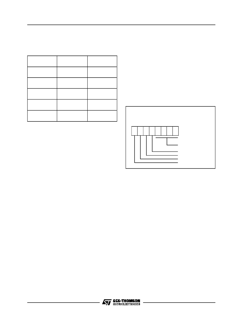
Figure 18. InterruptOption Register
D7.
Not used.
EL1.
This is the Edge/Level selection bit of inter-
rupt #1.When set to one,the interruptisgenerated
on low level of the related signal; when clearedto
zero,theinterruptisgenerated onfalling edge.The
bit is cleared to zeroafter reset.
ES2.
This is the edge selectionbit on interrupt#2.
ThisbitisusedontheST6369deviceswithon-chip
OSDgenerator for VSYNCdetection.
GEN.
Thisistheglobalenablebit.Whensettooneall
interruptsaregloballyenabled;whenthisbitiscleared
tozeroall interruptsaredisabled(excludingNMI).
D3 - D0.
These bits are not used.
Interrupt Source
Associated
Vector
Vector Address
PC6/IRIN
Pin (1)
Interrupt
Vector # 0 (NMI)
0FFCH-0FFDH
Timer2
Interrupt
Vector # 1
0FF6H-0FF7H
Vsync
Interrupt
Vector # 2
0FF4H-0FF5H
Timer1
Interrupt
Vector # 3
0FF2H-0FF3H
PC4/PWRIN
Interrupt
Vector # 4
0FF0H-0FF1H
Note
: 1. This pin isassociated with the NMI Interrupt Vector
Table 6. Interrupt Vectors/Sources
Relationships
INTERRUPT
(Continued)
IOR
InterruptOption Register
(C8H, Write Only)
D7 D6 D5 D4 D3 D2 D1 D0
Unused
Unused
GEN =GlobalEnable Bit
ES2 =Edge SelectionBit
EL1 = EdgeLevelSelection Bit
ST6369
16/67
相關(guān)PDF資料 |
PDF描述 |
|---|---|
| ST700C12L0 | PHASE CONTROL THYRISTORS Hockey Puk Version |
| ST700C12L0L | PHASE CONTROL THYRISTORS Hockey Puk Version |
| ST700C12L1 | PHASE CONTROL THYRISTORS Hockey Puk Version |
| ST700C | PHASE CONTROL THYRISTORS Hockey Puk Version |
| ST700C12L2L | PHASE CONTROL THYRISTORS Hockey Puk Version |
相關(guān)代理商/技術(shù)參數(shù) |
參數(shù)描述 |
|---|---|
| ST63E73J5D1 | 制造商:STMICROELECTRONICS 制造商全稱(chēng):STMicroelectronics 功能描述:8-BIT ROM/OTP/EPROM MCUs FOR DIGITALLY CONTROLLED MULTISYNC/MULTISTANDARD MONITORS |
| ST63E85D1 | 制造商:STMICROELECTRONICS 制造商全稱(chēng):STMicroelectronics 功能描述:8-BIT MCUs WITH ON-SCREEN-DISPLAY FOR TV TUNING |
| ST63E85D1/XX | 制造商:未知廠家 制造商全稱(chēng):未知廠家 功能描述:8-Bit Microcontroller |
| ST63E87D1 | 制造商:STMICROELECTRONICS 制造商全稱(chēng):STMicroelectronics 功能描述:8-BIT MCUs WITH ON-SCREEN-DISPLAY FOR TV TUNING |
| ST63E87D1/XX | 制造商:未知廠家 制造商全稱(chēng):未知廠家 功能描述:8-Bit Microcontroller |
發(fā)布緊急采購(gòu),3分鐘左右您將得到回復(fù)。