- 您現(xiàn)在的位置:買賣IC網(wǎng) > PDF目錄385870 > ST63E69D1 (意法半導(dǎo)體) 8-BIT HCMOS MCU FOR DIGITAL CONTROLLED MULTI FREQUENCYMONITOR PDF資料下載
參數(shù)資料
| 型號(hào): | ST63E69D1 |
| 廠商: | 意法半導(dǎo)體 |
| 英文描述: | 8-BIT HCMOS MCU FOR DIGITAL CONTROLLED MULTI FREQUENCYMONITOR |
| 中文描述: | 8位HCMOS單片機(jī)的數(shù)控多FREQUENCYMONITOR |
| 文件頁(yè)數(shù): | 43/71頁(yè) |
| 文件大小: | 584K |
| 代理商: | ST63E69D1 |
第1頁(yè)第2頁(yè)第3頁(yè)第4頁(yè)第5頁(yè)第6頁(yè)第7頁(yè)第8頁(yè)第9頁(yè)第10頁(yè)第11頁(yè)第12頁(yè)第13頁(yè)第14頁(yè)第15頁(yè)第16頁(yè)第17頁(yè)第18頁(yè)第19頁(yè)第20頁(yè)第21頁(yè)第22頁(yè)第23頁(yè)第24頁(yè)第25頁(yè)第26頁(yè)第27頁(yè)第28頁(yè)第29頁(yè)第30頁(yè)第31頁(yè)第32頁(yè)第33頁(yè)第34頁(yè)第35頁(yè)第36頁(yè)第37頁(yè)第38頁(yè)第39頁(yè)第40頁(yè)第41頁(yè)第42頁(yè)當(dāng)前第43頁(yè)第44頁(yè)第45頁(yè)第46頁(yè)第47頁(yè)第48頁(yè)第49頁(yè)第50頁(yè)第51頁(yè)第52頁(yè)第53頁(yè)第54頁(yè)第55頁(yè)第56頁(yè)第57頁(yè)第58頁(yè)第59頁(yè)第60頁(yè)第61頁(yè)第62頁(yè)第63頁(yè)第64頁(yè)第65頁(yè)第66頁(yè)第67頁(yè)第68頁(yè)第69頁(yè)第70頁(yè)第71頁(yè)
14-BIT PWM D/A CONVERTER
The ST6369 PWM D/A CONVERTER (HDA) is
composed of a 14-bit counterthat allows the con-
version of the digital contentin an analog voltage,
available at the HDA output pin, by using Pulse
Width Modification (PWM), and Bit Rate Multiplier
(BRM) techniques.
The tuning word consists of a 14-bit word con-
tained inthe registersHDADATA1(location 0EEH)
and HDADATA2 (location 0EFH). Coarse tuning
(PWM) isperformedusing thesevenMSBits,while
fine tuning (BRM) is performed using the data in
the seven LSBits.With all zerosloaded the output
is zero;asthe tuningvoltageincreases from all ze-
ros, the number of pulses in one period increasto
128 with all pulses being the same width. For val-
ues larger than 128, the PWM takes over and the
number of pulses in one period remains constant
at 128, but the width changes.At the other end of
the scale, when almost all ones are loaded, the
pulses will startto link together and the number of
pulses will decrease. When all ones are loaded,
the outputwill be almost100% high but will have a
low pulse (1/16384 of the high pulse).
OutputDetails
Inside the on-chip D/A CONVERTER are included
the registerlatches,areferencecounter,PWMand
BRM control circuitry. In the ST6369 the clock for
the 14-bit reference counteris 2MHz derived from
the 8MHz system clock. From the circuit point of
view, the seven most significant bits control the
coarse tuning,while the seven leastsignificant bits
control the fine tuning. From the application and
software point of view, the 14 bits can be consid-
ered asone binary number.
As already mentionedthe coarse tuningconsistsof
a PWMsignal with128 steps; we can considerthe
fine tuningto cover128 coarse tuning cycles.The
addition of pulses is described in the following Ta-
ble.
FIne Tuning
(7 LSB)
N
°
of Pulses added at
the following cycles
(0...127)
0000001
64
0000010
32, 96
0000100
16, 48, 80, 112
0001000
8, 24, ....104, 120
0010000
4, 12, ....116, 124
0100000
2, 6, .....122, 126
1000000
1, 3, .....125, 127
Table 11. Fine Tuning PulseAddition
The HDA outputpin has astandard drivepush-pull
output configuration.
HDA Tuning Cell Registers
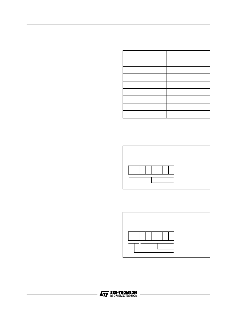
Figure 48. HDA Data Register 1
D7-D0.
These are the 8 least significant HDA data
bits. Bit 0 is the LSB.This registeris undefined on
reset.
Figure 49. HDA Data Register 2
D7-D6.
Thesebits are not used.
D5-D0.
These are the 6 mostsignificant HDA data
bits. Bit5 is the MSB. This registeris undefined on
reset.
HDADR1
HDA Data Register 1
(0EEH, Write only)
D7 D6 D5 D4 D3 D2 D1 D0
HDA Data Bits(LSB)
HDADR2
HDA Data Register 2
(0EFH, Write only)
D7 D6 D5 D4 D3 D2 D1 D0
HDA Data Bits(LSB)
Unused
ST6369
39/67
相關(guān)PDF資料 |
PDF描述 |
|---|---|
| ST700C12L0 | PHASE CONTROL THYRISTORS Hockey Puk Version |
| ST700C12L0L | PHASE CONTROL THYRISTORS Hockey Puk Version |
| ST700C12L1 | PHASE CONTROL THYRISTORS Hockey Puk Version |
| ST700C | PHASE CONTROL THYRISTORS Hockey Puk Version |
| ST700C12L2L | PHASE CONTROL THYRISTORS Hockey Puk Version |
相關(guān)代理商/技術(shù)參數(shù) |
參數(shù)描述 |
|---|---|
| ST63E73J5D1 | 制造商:STMICROELECTRONICS 制造商全稱:STMicroelectronics 功能描述:8-BIT ROM/OTP/EPROM MCUs FOR DIGITALLY CONTROLLED MULTISYNC/MULTISTANDARD MONITORS |
| ST63E85D1 | 制造商:STMICROELECTRONICS 制造商全稱:STMicroelectronics 功能描述:8-BIT MCUs WITH ON-SCREEN-DISPLAY FOR TV TUNING |
| ST63E85D1/XX | 制造商:未知廠家 制造商全稱:未知廠家 功能描述:8-Bit Microcontroller |
| ST63E87D1 | 制造商:STMICROELECTRONICS 制造商全稱:STMicroelectronics 功能描述:8-BIT MCUs WITH ON-SCREEN-DISPLAY FOR TV TUNING |
| ST63E87D1/XX | 制造商:未知廠家 制造商全稱:未知廠家 功能描述:8-Bit Microcontroller |
發(fā)布緊急采購(gòu),3分鐘左右您將得到回復(fù)。