- 您現(xiàn)在的位置:買賣IC網(wǎng) > PDF目錄371180 > T8534 T8533/34 Quad Programmable Line Card Signal Processor PDF資料下載
參數(shù)資料
| 型號: | T8534 |
| 英文描述: | T8533/34 Quad Programmable Line Card Signal Processor |
| 中文描述: | T8533/34四線卡可編程信號處理器 |
| 文件頁數(shù): | 16/48頁 |
| 文件大小: | 890K |
| 代理商: | T8534 |
第1頁第2頁第3頁第4頁第5頁第6頁第7頁第8頁第9頁第10頁第11頁第12頁第13頁第14頁第15頁當(dāng)前第16頁第17頁第18頁第19頁第20頁第21頁第22頁第23頁第24頁第25頁第26頁第27頁第28頁第29頁第30頁第31頁第32頁第33頁第34頁第35頁第36頁第37頁第38頁第39頁第40頁第41頁第42頁第43頁第44頁第45頁第46頁第47頁第48頁

Preliminary Data Sheet
July 2001
Signal Processor
T8533/34 Quad Programmable Line Card
16
Agere Systems Inc.
Functional Description
(continued)
The Control Interface
(continued)
Read Command
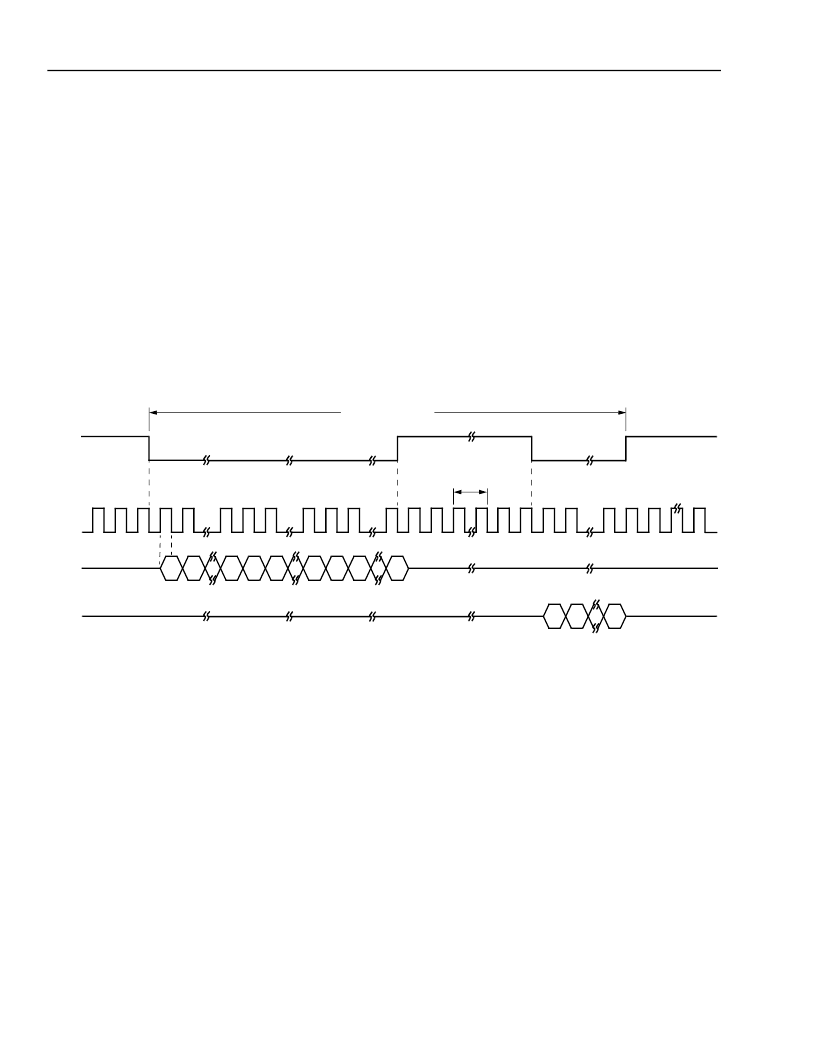
The normal flow of information to the master controller is always in response to a read command. All control mem-
ory locations are accessed in 8-bit bytes. All read commands from the master controller require a response from
the addressed codec. It is the responsibility of the master controller to ensure that only one device is transmitting
on the serial interface line at any one time. The master controller also must ensure that the CS lead goes high after
transferring the 3-byte sequence used to initiate the read, and then it goes low again for the response. In this case,
it should be noted that the device expects the second time CS goes low that data is to be sent to the master; thus,
it does not interpret the DI lead as containing a valid instruction during that CS excursion and a write during this
time is not recommended. Note also that the CS lead must allow the number of bytes sent in a read command to
be transferred before a subsequent command can be received by the codec. Figures 11—14 illustrate normal or
byte-by-byte operation with continuous or gapped DCLKs. Like a write command, transitions, not frequency, are
critical with regard to gapped DCLK operation.
0079
* Provide sufficient wait time to access read data. Provide sufficient DCLK cycles to effectively wait
≥
1.5
μ
s after the second full DCLK cycle
and before the second to last full DCLK cycle. DCLK operation of 4.096 MHz would require 10 cycles of DCLK between LENGTH and DATA.
The first two DCLK cycles, when CS goes high, processes the command. A wait is then required to access the read data. Two final DCLK
cycles are required to process the read data.
Two or more DCLK cycles are required before the start of a new command frame.
Note: Data field length of 1 shown.
Figure 11. Read Operation, Normal Mode (Continuous DCLK)
COMMAND FRAME
0
1
7
0
1
7
CS
DCLK
DI
COMMAND
START ADDRESS
DATA
0
1
7
0
1
7
0
1
7
LENGTH
0
1
7
0
1
7
0
1
7
DO
WAIT
≥
1.5
μ
s
*
相關(guān)PDF資料 |
PDF描述 |
|---|---|
| T8535B | T8535B/T8536B Quad Programmable Codec |
| T8536B | T8535B/T8536B Quad Programmable Codec |
| T8538B | T8538B Quad Programmable Codec |
| T923CFAA | T92-Type 10 Gbits/s 1300 nm Uncooled DFB Laser Transmitter |
| T923WFAA | T92-Type 10 Gbits/s 1300 nm Uncooled DFB Laser Transmitter |
相關(guān)代理商/技術(shù)參數(shù) |
參數(shù)描述 |
|---|---|
| T8535B | 制造商:AGERE 制造商全稱:AGERE 功能描述:T8535B/T8536B Quad Programmable Codec |
| T8536B | 制造商:AGERE 制造商全稱:AGERE 功能描述:T8535B/T8536B Quad Programmable Codec |
| T8538B | 制造商:AGERE 制造商全稱:AGERE 功能描述:T8538B Quad Programmable Codec |
| T85471G | 制造商:BITECH 制造商全稱:Bi technologies 功能描述:Thick Film Super Low Profile SIP Resistor Networks |
| T85471J | 制造商:BITECH 制造商全稱:Bi technologies 功能描述:Thick Film Super Low Profile SIP Resistor Networks |
發(fā)布緊急采購,3分鐘左右您將得到回復(fù)。