- 您現(xiàn)在的位置:買賣IC網(wǎng) > PDF目錄300083 > V59C1G01408QAJ37E (PROMOS TECHNOLOGIES INC) 256M X 4 DDR DRAM, 0.5 ns, PBGA68 PDF資料下載
參數(shù)資料
| 型號(hào): | V59C1G01408QAJ37E |
| 廠商: | PROMOS TECHNOLOGIES INC |
| 元件分類: | DRAM |
| 英文描述: | 256M X 4 DDR DRAM, 0.5 ns, PBGA68 |
| 封裝: | ROHS COMPLIANT, FBGA-68 |
| 文件頁(yè)數(shù): | 53/79頁(yè) |
| 文件大小: | 1029K |
| 代理商: | V59C1G01408QAJ37E |
第1頁(yè)第2頁(yè)第3頁(yè)第4頁(yè)第5頁(yè)第6頁(yè)第7頁(yè)第8頁(yè)第9頁(yè)第10頁(yè)第11頁(yè)第12頁(yè)第13頁(yè)第14頁(yè)第15頁(yè)第16頁(yè)第17頁(yè)第18頁(yè)第19頁(yè)第20頁(yè)第21頁(yè)第22頁(yè)第23頁(yè)第24頁(yè)第25頁(yè)第26頁(yè)第27頁(yè)第28頁(yè)第29頁(yè)第30頁(yè)第31頁(yè)第32頁(yè)第33頁(yè)第34頁(yè)第35頁(yè)第36頁(yè)第37頁(yè)第38頁(yè)第39頁(yè)第40頁(yè)第41頁(yè)第42頁(yè)第43頁(yè)第44頁(yè)第45頁(yè)第46頁(yè)第47頁(yè)第48頁(yè)第49頁(yè)第50頁(yè)第51頁(yè)第52頁(yè)當(dāng)前第53頁(yè)第54頁(yè)第55頁(yè)第56頁(yè)第57頁(yè)第58頁(yè)第59頁(yè)第60頁(yè)第61頁(yè)第62頁(yè)第63頁(yè)第64頁(yè)第65頁(yè)第66頁(yè)第67頁(yè)第68頁(yè)第69頁(yè)第70頁(yè)第71頁(yè)第72頁(yè)第73頁(yè)第74頁(yè)第75頁(yè)第76頁(yè)第77頁(yè)第78頁(yè)第79頁(yè)
57
ProMOS TECHNOLOGIES
V59C1G01(408/808/168)QA
V59C1G01(408/808/168)QA Rev. 1.2 April 2008
AC & DC operating conditions
Operation or timing that is not specified is illegal, and after such an event, in order to guarantee proper operation, the
DRAM must be powered down and then restarted through the speechified initialization sequence before normal
operation can continue.
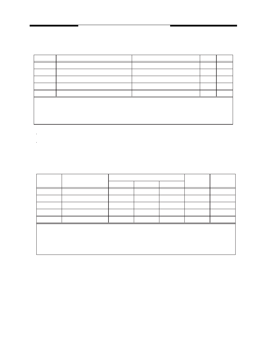
Absolute maximum DC ratings
Symbol
Parameter
Rating
Units
Notes
VDD
Voltage on VDD pin relative to Vss
- 1.0 V ~ 2.3 V
V
1,3
VDDQ
Voltage on VDDQ pin relative to Vss
- 0.5 V ~ 2.3 V
V
1,3
VDDL
Voltage on VDDL pin relative to Vss
- 0.5 V ~ 2.3 V
V
1,3
V
IN
, VOUT
Voltage on any pin relative to Vss
- 0.5 V ~ 2.3 V
V
1
T
STG
Storage Temperature
-55 to +100
C
1, 2
NOTE 1
Stresses greater than those listed under “Absolute Maximum Ratings” may cause permanent damage to the device. This is a stress rating
only and functional operation of the device at these or any other conditions above those indicated in the operational sections of this specification is
not implied. Exposure to absolute maximum rating conditions for extended periods may affect reliability
NOTE 2
Storage Temperature is the case surface temperature on the center/top side of the DRAM. For the measurement conditions, please refer to
JESD51-2 standard.
NOTE 3
When VDD and VDDQ and VDDL are less than 500 mV, Vref may be equal to or less than 300 mV.
Recommended DC operating conditions (SSTL_1.8)
Symbol
Parameter
Rating
Units
Notes
Min.
Typ.
Max.
VDD
Supply Voltage
1.7
1.8
1.9
V
1
VDDL
Supply Voltage for DLL
1.7
1.8
1.9
V
5
VDDQ
Supply Voltage for Output
1.7
1.8
1.9
V
1, 5
VREF
Input Reference Voltage
0.49 x VDDQ
0.50 x VDDQ
0.51 x VDDQ
mV
2. 3
VTT
Termination Voltage
VREF - 0.04
VREF
VREF + 0.04
V
4
NOTE 1 There is no specific device VDD supply voltage requirement for SSTL_18 compliance. However under all conditions VDDQ must be less
than or equal to VDD.
NOTE 2
The value of VREF may be selected by the user to provide optimum noise margin in the system. Typically the value of VREF is expected
to be about 0.5 x VDDQ of the transmitting device and VREF is expected to track variations in VDDQ.
NOTE 3
Peak to peak ac noise on VREF may not exceed +/-2 % VREF(dc).
NOTE 4
VTT of transmitting device must track VREF of receiving device.
NOTE 5
VDDQ tracks with VDD, VDDL tracks with VDD. AC parameters are measured with VDD, VDDQ and VDDDL tied together
相關(guān)PDF資料 |
PDF描述 |
|---|---|
| V59C1G01408QAJ37I | 256M X 4 DDR DRAM, 0.5 ns, PBGA68 |
| V5D010EB4D | SNAP ACTING/LIMIT SWITCH, SPDT, MOMENTARY, 0.5A, 125VDC, 4.4mm, PANEL MOUNT |
| V5F110CB | SNAP ACTING/LIMIT SWITCH, SPDT, MOMENTARY, PANEL MOUNT |
| V5PNF | CABLE TERMINATED, FEMALE, N CONNECTOR, THREAD-IN STUB SELF-FLARE |
| V5T110TB3 | SNAP ACTING/LIMIT SWITCH, SPDT, MOMENTARY, 0.6A, 125VDC, 2.4mm, PANEL MOUNT |
相關(guān)代理商/技術(shù)參數(shù) |
參數(shù)描述 |
|---|---|
| V5A010CB | 制造商:Honeywell Sensing and Control 功能描述:MICROSWITCH V5 PIN PLUNGER |
| V5A010CB | 制造商:Honeywell Sensing and Control 功能描述:MICROSWITCH V5 PIN PLUNGER |
| V5A010CB4D | 制造商:Honeywell Sensing and Control 功能描述:MICROSWITCH V5 ROLLER LEVER |
| V5A010CB4D | 制造商:Honeywell Sensing and Control 功能描述:MICROSWITCH V5 ROLLER LEVER |
| V5A010CB4E | 制造商:Honeywell Sensing and Control 功能描述:MICROSWITCH V5 ROLLER LEVER |
發(fā)布緊急采購(gòu),3分鐘左右您將得到回復(fù)。