- 您現(xiàn)在的位置:買賣IC網(wǎng) > PDF目錄300083 > V59C1G01408QAJ37E (PROMOS TECHNOLOGIES INC) 256M X 4 DDR DRAM, 0.5 ns, PBGA68 PDF資料下載
參數(shù)資料
| 型號: | V59C1G01408QAJ37E |
| 廠商: | PROMOS TECHNOLOGIES INC |
| 元件分類: | DRAM |
| 英文描述: | 256M X 4 DDR DRAM, 0.5 ns, PBGA68 |
| 封裝: | ROHS COMPLIANT, FBGA-68 |
| 文件頁數(shù): | 63/79頁 |
| 文件大小: | 1029K |
| 代理商: | V59C1G01408QAJ37E |
第1頁第2頁第3頁第4頁第5頁第6頁第7頁第8頁第9頁第10頁第11頁第12頁第13頁第14頁第15頁第16頁第17頁第18頁第19頁第20頁第21頁第22頁第23頁第24頁第25頁第26頁第27頁第28頁第29頁第30頁第31頁第32頁第33頁第34頁第35頁第36頁第37頁第38頁第39頁第40頁第41頁第42頁第43頁第44頁第45頁第46頁第47頁第48頁第49頁第50頁第51頁第52頁第53頁第54頁第55頁第56頁第57頁第58頁第59頁第60頁第61頁第62頁當(dāng)前第63頁第64頁第65頁第66頁第67頁第68頁第69頁第70頁第71頁第72頁第73頁第74頁第75頁第76頁第77頁第78頁第79頁
66
V59C1G01(408/808/168)QA Rev. 1.2 April 2008
ProMOS TECHNOLOGIES
V59C1G01(408/808/168)QA
DDR2 SDRAM Default Output Driver V–I Characteristics
DDR2 SDRAM output driver characteristics are defined for full strength default operation as selected by
the EMRS1 bits A7-A9 = ‘111’. Figures 1 and 2 show the driver characteristics graphically, and tables 1 and
2 show the same data in tabular format suitable for input into simulation tools. The driver characteristics
evaluation conditions are:
Nominal Default 25 oC (T case), VDDQ = 1.8 V, typical process
Minimum TBD oC (T case), VDDQ = 1.7 V, slow–slow process
Maximum 0 oC (T case), VDDQ = 1.9 V, fast–fast process
Default Output Driver Characteristic Curves Notes:
1) The full variation in driver current from minimum to maximum process, temperature, and voltage will
lie within the outer bounding lines of the V–I curve of figures 1 and 2.
2) It is recommended that the ”typical” IBIS V–I curve lie within the inner bounding lines of the V–I curves
of figures 1 and 2.
Table 3.
Full Strength Calibrated Pulldown Driver Characteristics
Table 4.
Full Strength Calibrated Pullup Driver Characteristics
DDR2 SDRAM Calibrated Output Driver V–I Characteristics
DDR2 SDRAM output driver characteristics are defined for full strength calibrated operation as selected by
the procedure outlined in the section of Off-Chip Driver (OCD) Impedance Adjustment. Tables 3 and 4
show the data in tabular format suitable for input into simulation tools. The nominal points represent a
device at exactly 18 ohms. The nominal low and nominal high values represent the range that can be
achieved with a maximum 1.5 ohm step size with no calibration error at the exact nominal conditions only
(i.e. perfect calibration procedure, 1.5 ohm maximum step size guaranteed by specification). Real system
calibration error needs to be added to these values. It must be understood that these V-I curves as repre-
sented here or in supplier IBIS models need to be adjusted to a wider range as a result of any system cali-
bration error. Since this is a system specific phenomena, it cannot be quantified here. The values in the
calibrated tables represent just the DRAM portion of uncertainty while looking at one DQ only. If the cali
-
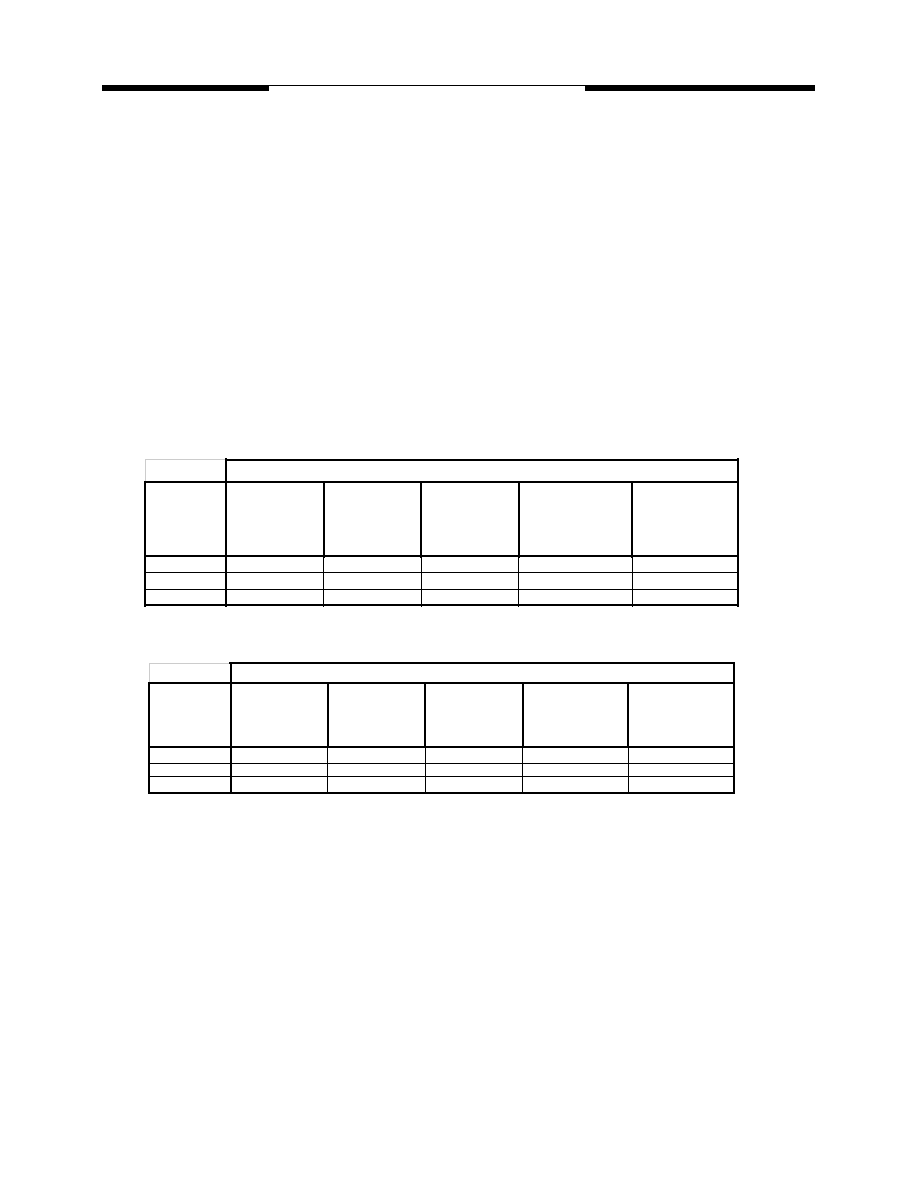
Calibrated Pulldow n Current (mA)
Voltage (V)
Nominal Minimum
(21 ohms)
Nominal Low
(18.75 ohms)
Nominal (18 ohms)
Nominal High
(17.2 ohms)
Nominal Maximum
(15 ohms)
0.2
9.5
10.7
11.5
11.8
13.3
0.3
14.3
16.0
16.6
17.4
20.0
0.4
18.7
21.0
21.6
23.0
27.0
Calibrated Pullup Current (mA)
Voltage (V)
Nominal Minimum
(21 ohms)
Nominal (18 ohms)
0.2
-9.5
-10.7
-11.4
-11.8
-13.3
0.3
-14.3
-16.0
-16.5
-17.4
-20.0
0.4
-18.7
-21.0
-21.2
-23.0
-27.0
Nominal Low
(18.75 ohms)
Nominal High
(17.2 ohms)
Nominal Maximum
(15 ohms)
相關(guān)PDF資料 |
PDF描述 |
|---|---|
| V59C1G01408QAJ37I | 256M X 4 DDR DRAM, 0.5 ns, PBGA68 |
| V5D010EB4D | SNAP ACTING/LIMIT SWITCH, SPDT, MOMENTARY, 0.5A, 125VDC, 4.4mm, PANEL MOUNT |
| V5F110CB | SNAP ACTING/LIMIT SWITCH, SPDT, MOMENTARY, PANEL MOUNT |
| V5PNF | CABLE TERMINATED, FEMALE, N CONNECTOR, THREAD-IN STUB SELF-FLARE |
| V5T110TB3 | SNAP ACTING/LIMIT SWITCH, SPDT, MOMENTARY, 0.6A, 125VDC, 2.4mm, PANEL MOUNT |
相關(guān)代理商/技術(shù)參數(shù) |
參數(shù)描述 |
|---|---|
| V5A010CB | 制造商:Honeywell Sensing and Control 功能描述:MICROSWITCH V5 PIN PLUNGER |
| V5A010CB | 制造商:Honeywell Sensing and Control 功能描述:MICROSWITCH V5 PIN PLUNGER |
| V5A010CB4D | 制造商:Honeywell Sensing and Control 功能描述:MICROSWITCH V5 ROLLER LEVER |
| V5A010CB4D | 制造商:Honeywell Sensing and Control 功能描述:MICROSWITCH V5 ROLLER LEVER |
| V5A010CB4E | 制造商:Honeywell Sensing and Control 功能描述:MICROSWITCH V5 ROLLER LEVER |
發(fā)布緊急采購,3分鐘左右您將得到回復(fù)。