- 您現(xiàn)在的位置:買賣IC網(wǎng) > PDF目錄359412 > VPC3200A (MICRONAS SEMICONDUCTOR HOLDING AG) Comb Filter Video Processor PDF資料下載
參數(shù)資料
| 型號(hào): | VPC3200A |
| 廠商: | MICRONAS SEMICONDUCTOR HOLDING AG |
| 元件分類: | 消費(fèi)家電 |
| 英文描述: | Comb Filter Video Processor |
| 中文描述: | SPECIALTY CONSUMER CIRCUIT, PQFP80 |
| 封裝: | PLASTIC, QFP-80 |
| 文件頁(yè)數(shù): | 55/78頁(yè) |
| 文件大小: | 1245K |
| 代理商: | VPC3200A |
第1頁(yè)第2頁(yè)第3頁(yè)第4頁(yè)第5頁(yè)第6頁(yè)第7頁(yè)第8頁(yè)第9頁(yè)第10頁(yè)第11頁(yè)第12頁(yè)第13頁(yè)第14頁(yè)第15頁(yè)第16頁(yè)第17頁(yè)第18頁(yè)第19頁(yè)第20頁(yè)第21頁(yè)第22頁(yè)第23頁(yè)第24頁(yè)第25頁(yè)第26頁(yè)第27頁(yè)第28頁(yè)第29頁(yè)第30頁(yè)第31頁(yè)第32頁(yè)第33頁(yè)第34頁(yè)第35頁(yè)第36頁(yè)第37頁(yè)第38頁(yè)第39頁(yè)第40頁(yè)第41頁(yè)第42頁(yè)第43頁(yè)第44頁(yè)第45頁(yè)第46頁(yè)第47頁(yè)第48頁(yè)第49頁(yè)第50頁(yè)第51頁(yè)第52頁(yè)第53頁(yè)第54頁(yè)當(dāng)前第55頁(yè)第56頁(yè)第57頁(yè)第58頁(yè)第59頁(yè)第60頁(yè)第61頁(yè)第62頁(yè)第63頁(yè)第64頁(yè)第65頁(yè)第66頁(yè)第67頁(yè)第68頁(yè)第69頁(yè)第70頁(yè)第71頁(yè)第72頁(yè)第73頁(yè)第74頁(yè)第75頁(yè)第76頁(yè)第77頁(yè)第78頁(yè)
ADVANCE INFORMATION
VPC 323xD, VPC 324xD
Micronas
55
Pin 29 – Supply Voltage, LLC Circuitry V
SUPLLC
This pin is connected with 68 nF to GND
LLC
Pin 30 – Ground, LLC Circuitry GND
LLC
Pins 31 to 34,37 to 40 – Luma Outputs Y7 – Y0 (Fig.
4–4)
These output pins carry the digital luminance data. The
outputs are clocked with the LLC1 clock. In ITUR656
mode the Y/C data is multiplexed and clocked with
LLC2 clock.
Pin 35– Ground, Luma Output Circuitry GND
Y
This pin is connected with 68 nF to GND
Y
Pin 36 – Supply Voltage, Luma Output Circuitry V
SUPY
Pins 41 to 44,47 to 50 – Chroma Outputs C7–C0 (Fig.
4–4) These outputs carry the digital CrCb chrominance
data. The outputs are clocked with the LL1 clock. The
CrCb data is sampled at half the clock rate and multi-
plexed. The CrCb multiplex is reset for each TV line. In
ITUR656 mode, the chroma outputs are tri-stated.
Pin 45 – Supply Voltage, Chroma Output Circuitry
V
SUPC
This pin is connected with 68 nF to GND
C
Pin 46 – Ground, Chroma Output Circuitry GND
C
Pin 51 – Ground, Sync Pad Circuitry GND
SY
Pin 52 – Supply Voltage, Sync Pad Circuitry V
SUPSY
This pin is connected with 47 nF/1.5 nF to GND
SY
Pin 53 – Interlace Output, INTLC (Fig. 4–4)
This pin supplies the interlace information, 0 indicates
first field, 1 indicates second field.
Pin 54 – Active Video Output, AVO (Fig. 4–4)
This pin indicates the active video output data. The
signal is clocked with the LLC1 clock.
Pin 55 – Front Sync/Horizontal Clamp Pulse, FSY/HC
(Fig. 4–4)
This signal can be used to clamp an external video sig-
nal, that is synchronous to the input signal. The timing
is programmable. In DIGIT3000 mode, this pin sup-
plies the front sync information.
Pin 56 – Main Sync/Horizontal Sync Pulse MSY/HS
(Fig. 4–4)
This pin supplies the horizontal sync pulse information
in line-locked mode. In DIGIT3000 mode, this pin is the
main sync input.
Pin 57 – Vertical Sync Pulse, VS (Fig. 4–4)
This pin supplies the vertical sync signal.
Pin 58 – Front-End/Back-End Data FPDAT (Fig. 4–5)
This pin interfaces to the DDP 3300A back-end pro-
cessor. The information for the deflection drives and for
the white drive control, i. e. the beam current limiter, is
transmitted by this pin.
Pin 59 – Standby Supply Voltage V
STDBY
In standby mode, only the clock oscillator is active,
GND
F
should be ground reference. Please activate
RESQ before powering-up other supplies
Pin 60 – CCU 5 MHz Clock Output CLK5 (Fig. 4–10)
This pin provides a clock frequency for the TV micro-
controller, e.g. a CCU 3000 controller. It is also used by
the DDP 3300A display controller as a standby clock.
Pins 62and 63 – XTAL1 Crystal Input and XTAL2 Crys-
tal Output (Fig. 4–7)
These pins are connected to an 20.25 MHz crystal
oscillator which is digitally tuned by integrated shunt
capacitances. The CLK20 and CLK5 clock signals are
derived from this oscillator. An external clock can be
fed into XTAL1. In this case, clock frequency adjust-
ment must be switched off.
Pin 65 – Ground, Analog Front-End GND
F
Pin 66 – Reference Voltage Top VRT (Fig. 4–8)
Via this pin, the reference voltage for the A/D converters
is decoupled. The pin is connected with 10
μ
F/47 nF to
the Signal Ground Pin.
Pin 67 – I
2
C Bus address select I2CSEL
This pin determines the I
2
C bus address of the IC.
Pin 68 – Signal GND for Analog Input ISGND (Fig. 4–
10) This is the high quality ground reference for the
video input signals.
Pin 69 – Supply Voltage, Analog Front-End V
SUPF
(Fig. 4–8)
This pin is connected with 220 nF/1.5 nF/390 pF to
GND
F
Pin 70 – Analog Video Output, VOUT (Fig. 4–6)
The analog video signal that is selected for the main
(luma, CVBS) ADC is output at this pin. An emitter fol-
lower is required at this pin.
Pin 71 – Chroma Input CIN (Fig. 4–9)
This pin is connected to the S-VHS chroma signal. A
resistive divider is used to bias the input signal to the
middle of the converter input range. CIN can only be
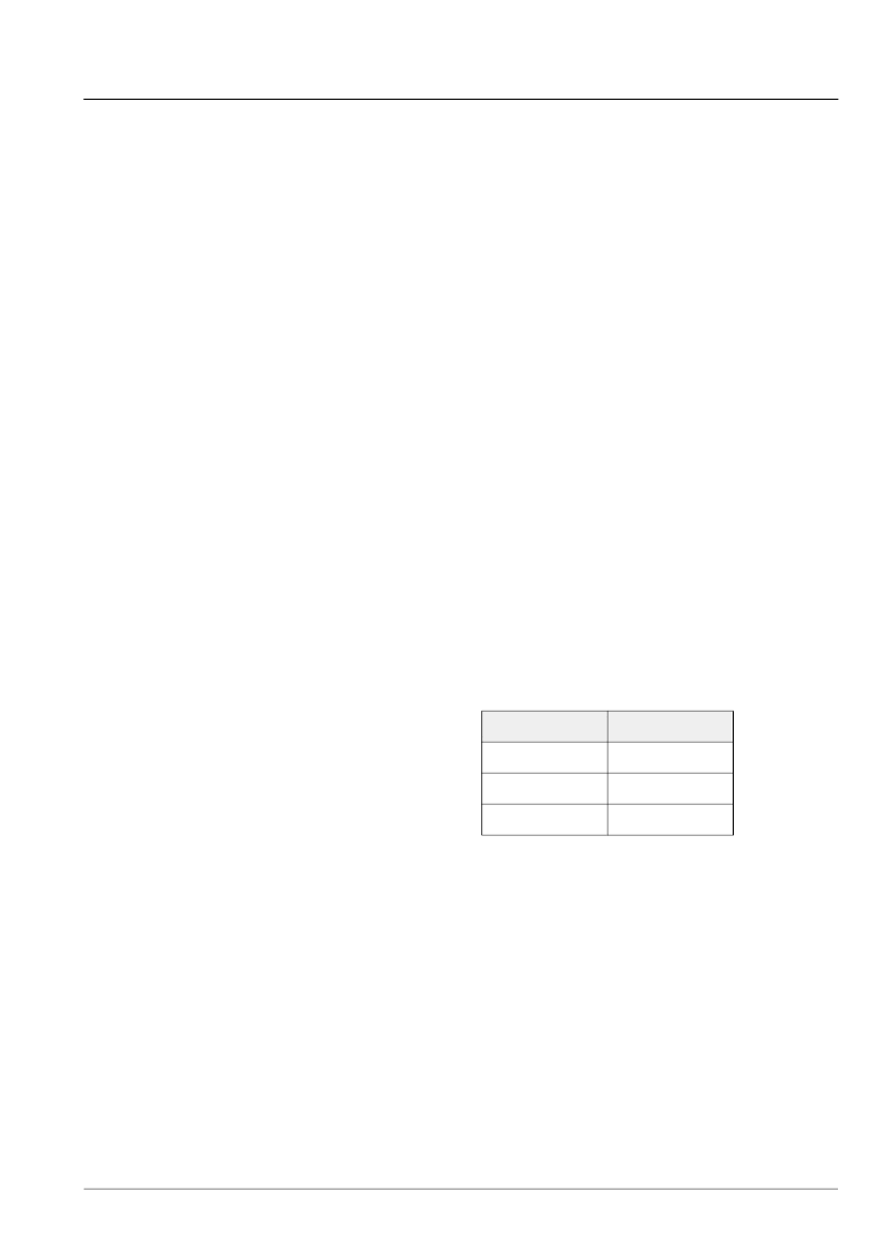
Table 4–1:
VPC32xxD I
2
C address select
I2CSEL
I
2
C Add.
GND
F
88/89 hex
VRT
8C/8D hex
V
SUPF
8E/8F hex
相關(guān)PDF資料 |
PDF描述 |
|---|---|
| VPDV1CHP | TRANSISTOR | MOSFET | P-CHANNEL | 100V V(BR)DSS | CHIP |
| VPDV2CHP | TRANSISTOR | MOSFET | P-CHANNEL | 240V V(BR)DSS | CHIP |
| VPE28W12D | Analog IC |
| VPE28W15D | Analog IC |
| VPF2805D | Analog IC |
相關(guān)代理商/技術(shù)參數(shù) |
參數(shù)描述 |
|---|---|
| VPC3200APSGP | 制造商:MICRONAS 功能描述:New |
| VPC3201A | 制造商:MICRONAS 制造商全稱:MICRONAS 功能描述:Comb Filter Video Processor |
| VPC3205C | 制造商:MICRONAS 制造商全稱:MICRONAS 功能描述:Comb Filter Video Processor |
| VPC3210A | 制造商:MICRONAS 制造商全稱:MICRONAS 功能描述:Comb Filter Video Processor |
| VPC3210B | 制造商:未知廠家 制造商全稱:未知廠家 功能描述:Consumer IC |
發(fā)布緊急采購(gòu),3分鐘左右您將得到回復(fù)。