- 您現在的位置:買賣IC網 > PDF目錄371305 > XA-H4 (NXP Semiconductors N.V.) Single-chip 16-bit microcontroller PDF資料下載
參數資料
| 型號: | XA-H4 |
| 廠商: | NXP Semiconductors N.V. |
| 英文描述: | Single-chip 16-bit microcontroller |
| 中文描述: | 單片16位微控制器 |
| 文件頁數: | 8/42頁 |
| 文件大小: | 225K |
| 代理商: | XA-H4 |
第1頁第2頁第3頁第4頁第5頁第6頁第7頁當前第8頁第9頁第10頁第11頁第12頁第13頁第14頁第15頁第16頁第17頁第18頁第19頁第20頁第21頁第22頁第23頁第24頁第25頁第26頁第27頁第28頁第29頁第30頁第31頁第32頁第33頁第34頁第35頁第36頁第37頁第38頁第39頁第40頁第41頁第42頁
Philips Semiconductors
Preliminary specification
XA-H4
Single-chip 16-bit microcontroller
1999 Sep 24
8
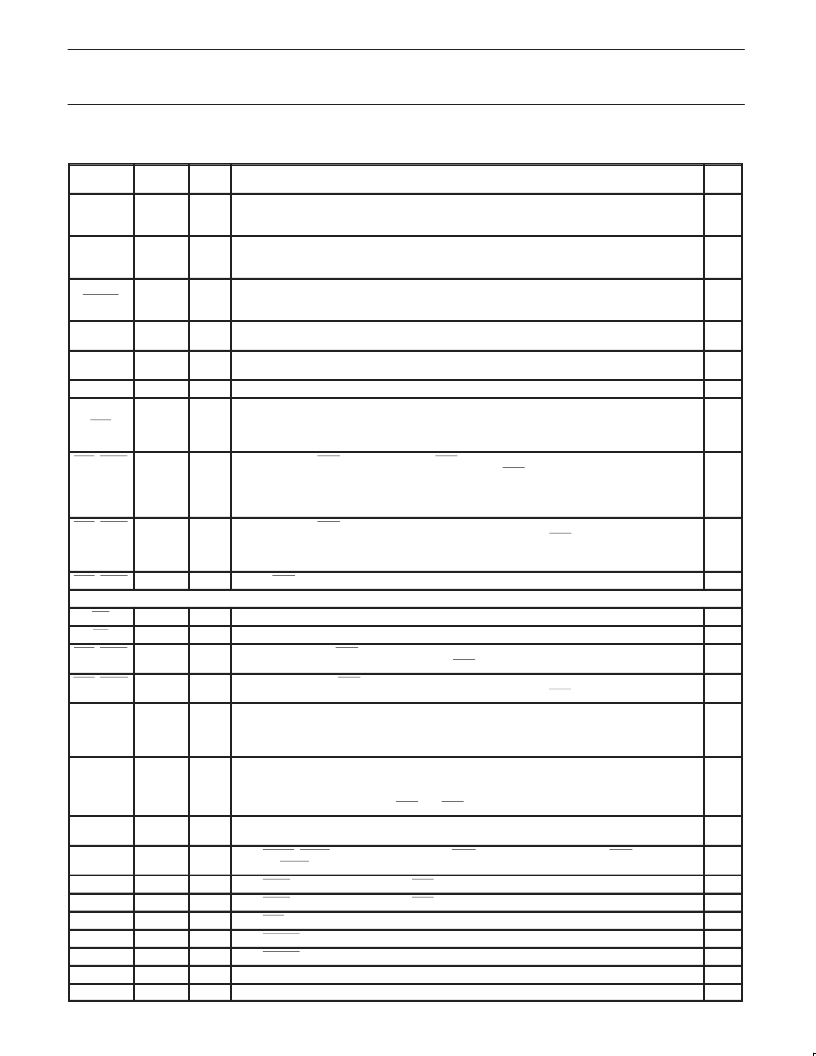
PIN DESCRIPTIONS
Mnemonic
Lqfp
Pin No.
1, 19, 28,
44, 59,
76, 88
Type
Name and Function
See
Note
V
SS
I
Ground:
0 V reference.
V
DD
2, 20, 29,
43, 62,
77, 89
I
Power Supply:
This is the power supply voltage for normal, idle, and power down operation.
ResetIn
55
I
Reset:
A low on this pin resets the microcontroller, causing I/O ports and peripherals to take on
their default states, and the processor to begin execution at the address contained in the reset
vector.
WAIT/
Size16
52
I
Wait/Size16:
During Reset, this input determines bus size for boot device (“1” = 16-bit boot
device; “0” = 8-bit.) During normal operation this is the Wait input (“1” = Wait; “0” = Proceed.)
Crystal 1:
Input to the inverting amplifier used in the oscillator circuit and input to the internal
clock generator circuits.
Crystal 2:
Output from the oscillator amplifier.
XTALIn
60
I
XTALOut
61
I
CS0
49
O
Chip Select 0:
This output provides the active low chip select to the boot device (usually ROM or
Flash.) It cannot be connected to DRAM. From reset, it is enabled and mapped to an address
range based at 000000h. It can be remapped by software to a higher base in the address map
(see the “Memory Interface” chapter in the XA-H4 User Manual)
CS1_RAS1
48
O
Chip Select 1
or
RAS1:
Chip Selects and RAS 1 through 5 come out of reset disabled. They can
be programmed to function as normal chip selects, or as RAS strobes to DRAM. CS1 can be
“swapped” with CS0 (see the SWAP operation and control bit in the “Memory Controller” chapter
of the XA-H4 User Manual) CS1 is usually mapped to be based at 000000h after the swap, but is
capable of being based anywhere in the 16 MB space.
CS2_RAS2
47
O
Chip Select 2
or
RAS2:
Active low Chip Selects CS1 through CS5 come out of reset disabled.
They can be programmed to function as normal chip selects, or as RAS strobes to DRAM. CS2
through CS5 are not used with the “SWAP” operation (see the “Memory Controller” chapter in the
XA-H4 User Manual) They are mappable to any region of the 16 MB address space.
CS3_RAS3
46
O
CS3 or RAS3:
See Chip Select 2 for description.
See Pins 56, 57 for 2 additional Chip Selects
WE
50
O
Write Enable:
Goes active low during all bus write cycles only.
OE
51
O
Output Enable:
Goes active low during all bus read cycles only.
BLE_CASL
54
O
Byte Low Enable
or
CAS_Low_Byte:
Goes active low during all bus cycles that access D7 – D0,
read or write, Generic or DRAM. Functions as CAS during DRAM cycles.
Byte High Enable
or
CAS_High_Byte:
Goes active low during all bus cycles that access data
bus lines D15 – D8, read or write, Generic or DRAM. Functions as CAS during DRAM cycles.
Clock Output:
This pin outputs a buffered version of the internal CPU clock. The clock output
may be used in conjunction with the external bus to synchronize WAIT state generators, etc. The
clock output may be disabled by software.
WARNING:
The capacitive loading on this output must not exceed 40 pf.
BHE_CASH
53
O
ClkOut
45
O
A19 – A0
24 – 21,
18 – 3
O
Address[19:0]:
These address lines output A19 – A0 during (SRAM, etc.) bus cycles.
DRAMS (H4 only) are connected only to pins 22, 21, 18 – 10 (pins A17 to A7; see user manual
“MIF Chapter” for connecting various DRAM sizes); the appropriate address values are
multiplexed onto these 11 pins for RAS and CAS during DRAM bus cycles.
D15 – D0
42 – 30,
27 – 25
I/O
Data[15:0]:
Bi-directional data bus, D15 – D0.
P0.0
90
I/O
P0.0_Sync0_BRG0:
Port 0 Bit 0, or USART0 Sync input or output, or USART0 BRG output, or
USART0
TxClk
output.
P0.1_RTS0:
Port 0 Bit 1, or USART0
RTS
(Request To Send) output.
1
P0.1
91
I/O
1
P0.2
92
I/O
P0.2_CTS0:
Port 0 Bit 2, or USART0 CTS (Clear To Send) input.
1
P0.3
93
I/O
P0.3_CD0:
Port 0 Bit 3, or USART0 Carrier Detect input.
1
P0.4
94
I/O
P0.4_TRClk0:
Port 0 Bit 4, or USART0 TR clock input.
1, 2
P0.5
95
I/O
P0.5_RTClk0:
Port 0 Bit 5, or USART0 RT clock input.
1, 2
P0.6
99
I/O
P0.6:
Port 0 Bit 6
1
P0.7
100
I/O
P0.7:
Port 0 Bit 7
1
相關PDF資料 |
PDF描述 |
|---|---|
| XACA04SPEC0304 | CONTROL STATION 4WAY |
| XACA06SPEC0305 | CONTROL STATION 6WAY |
| XACA215 | FERNSTEUEREINHEIT |
| XALB222 | WIPPSCHALTER ZB2 STEUERGEHAEUSE TASTEN 2 |
| XAITD-100 | Delay Line |
相關代理商/技術參數 |
參數描述 |
|---|---|
| XAI.50V2200 | 制造商:Xicon Passive Components 功能描述: |
| XAIR1-3402-101B | 制造商:Advantech Co Ltd 功能描述:CARRIER BOARD, AIR PRODUCTS 3402-101B3 - Bulk |
| XAIR1-3402-CARTON | 制造商:Advantech Co Ltd 功能描述:D-AIR01-SOM7562-01 - OUTER CARTON - Bulk |
| XAITD-100 | 制造商:RHOMBUS-IND 制造商全稱:Rhombus Industries Inc. 功能描述:XAITD Series FAST / TTL Buffered 10-Tap Delay Modules |
| XAITD-100G | 制造商:RHOMBUS-IND 制造商全稱:Rhombus Industries Inc. 功能描述:XAITD Series FAST / TTL Buffered 10-Tap Delay Modules |
發(fā)布緊急采購,3分鐘左右您將得到回復。