- 您現(xiàn)在的位置:買賣IC網(wǎng) > PDF目錄376461 > XRT73L04 (Exar Corporation) 4 Channel E3/DS3/STS-1 Line Interface Unit(4通道 E3/DS3/STS-1線接口單元) PDF資料下載
參數(shù)資料
| 型號(hào): | XRT73L04 |
| 廠商: | Exar Corporation |
| 英文描述: | 4 Channel E3/DS3/STS-1 Line Interface Unit(4通道 E3/DS3/STS-1線接口單元) |
| 中文描述: | 4頻道E3/DS3/STS-1線路接口單元(4通道E3/DS3/STS-1線接口單元) |
| 文件頁數(shù): | 26/62頁 |
| 文件大小: | 781K |
| 代理商: | XRT73L04 |
第1頁第2頁第3頁第4頁第5頁第6頁第7頁第8頁第9頁第10頁第11頁第12頁第13頁第14頁第15頁第16頁第17頁第18頁第19頁第20頁第21頁第22頁第23頁第24頁第25頁當(dāng)前第26頁第27頁第28頁第29頁第30頁第31頁第32頁第33頁第34頁第35頁第36頁第37頁第38頁第39頁第40頁第41頁第42頁第43頁第44頁第45頁第46頁第47頁第48頁第49頁第50頁第51頁第52頁第53頁第54頁第55頁第56頁第57頁第58頁第59頁第60頁第61頁第62頁
XRT73L04
4 CHANNEL DS3/E3/STS-1 LINE INTERFACE UNIT
REV. P1.0.5
á
PRELIMINARY
22
SYSTEM DESCRIPTION
A functional block diagram of the XRT73L04 E3/DS3/
STS-1 Transceiver IC is presented in Figure 10. The
XRT73L04 contains four separate channels with
three distinct sections:
The Transmit Section - Channels 0, 1, 2, and 3
The Receive Section - Channels 0, 1, 2, and 3
The Microprocessor Serial Interface Section
THE TRANSMIT SECTION - CHANNELS 0, 1, 2,
AND 3
The Transmit Section, within each Channel, accepts
TTL/CMOS level signals from the Terminal Equip-
ment in either a Single-Rail or Dual-Rail format. The
Transmit Section then takes this data and does the
following:
Encode this data into the B3ZS format if the DS3 or
SONET STS-1 Modes has been selected or into
the HDB3 format if the E3 Mode has been selected.
Convert the CMOS level B3ZS or HDB3 encoded
data into pulses with shapes that are compliant with
the various industry standard pulse template
requirements.
Drive these pulses onto the line via the TTIP(n) and
TRing(n) output pins across a 1:1 Transformer.
N
OTE
:
The Transmit Section drives a "1" (or a Mark) onto
the line by driving either a positive or negative polarity pulse
across the 1:1 Transformer within a given bit period. The
Transmit Section drives a "0" (or a Space) onto the line by
driving no pulse onto the line.
THE RECEIVE SECTION - CHANNELS 0, 1, 2 AND
3
The Receive Section, within each Channel, receives
a bipolar signal from the line via the RTIP and RRing
signals through a 1:1 Transformer or 0.01μF Capaci-
tor.
The recovered clock and data outputs to the Local
Terminal Equipment in the form of CMOS level sig-
nals via the RPOS(n), RNEG(n) and RxClk(n) output
pins.
THE MICROPROCESSOR SERIAL INTERFACE
The XRT73L04 can be configured to operate in either
the Hardware Mode or the HOST Mode.
The XRT73L04 contains four identical channels. The
Microprocessor Interface Inputs are common to all
channels. The descriptions that follow refer to Chan-
nel(n) where (n) represents channel 0, 1, 2 or 3.
a. Operating in the Hardware Mode
When the XRT73L04 is operating in the Hardware
Mode, then the following is true:
1.
The Microprocessor Serial Interface block is dis-
abled.
2.
The XRT73L04 is configured via input pin set-
tings.
The XRT73L04 can be configured to operate in the
Hardware Mode by tying the HOST/(HW) input pin to
GND.
Each of the pins associated with the Microprocessor
Serial Interface takes on their alternative role as de-
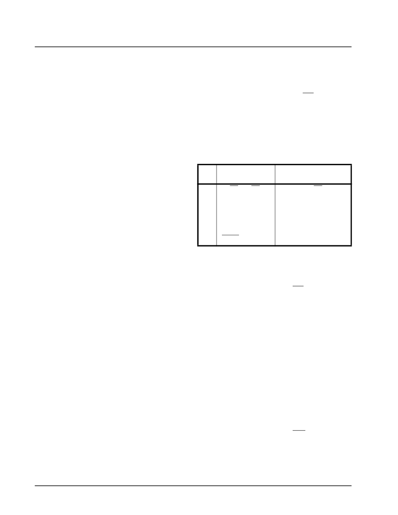
fined inTable 1.
T
ABLE
1: R
OLE
OF
M
ICROPROCESSOR
S
ERIAL
I
NTERFACE
PINS
WHEN
THE
XRT73L04
IS
OPERATING
IN
THE
H
ARDWARE
M
ODE
When the XRT73L04 is operating in the Hardware
Mode, all of the remaining input pins become active.
b. Operating in the HOST Mode
The XRT73L04 can be configured to operate in the
HOST Mode by tying the HOST/(HW) input pin to
VDD.
When the XRT73L04 is operating in the HOST Mode,
then the following is true.
1.
The Microprocessor Serial Interface block is
enabled. Writing the appropriate data into the
on-chip Command Registers makes many config-
uration selections.
2.
All of the following input pins are disabled and
should be connected to ground:
Pins 43, 44, 137 & 138 - TxLEV(n)
Pins 45, 46, 135 & 136 TAOS(n)
Pin 82, 90, 91 & 99 - REQEN(n)
Pin 77, 85, 96 & 104 - RLB(n)
Pin 76, 84, 97 & 105 - LLB(n)
Pin 107 & 108 - E3_Ch(n)
Pin 73, 83, 98 &106 - STS-1/DS3_Ch(n)
In HOST Mode Operation, the TxOFF input pins can
be used to turn on or turn off the Transmit Output
Drivers within all Channels concurrently. The intent
behind this feature is to permit a system designed for
P
IN
#
P
IN
N
AME
F
UNCTION
,
WHILE
IN
HARDWARE
MODE
69
CS/(SR/DR)
(SR/DR)
70
SClk/(RxOFF)
RxOFF
71
SDI/(E3_Ch1)
E3_Ch1
72
SDO/(E3_Ch0)
E3_Ch0
110
REGR/(RxClkINV)
RxClkINV
相關(guān)PDF資料 |
PDF描述 |
|---|---|
| XRT73L06 | SIX CHANNEL E3/DS3/STS-1 LINE INTERFACE UNIT |
| XRT73L06IB | SIX CHANNEL E3/DS3/STS-1 LINE INTERFACE UNIT |
| XRT73LC00A | E3/DS3/STS-1 LINE INTERFACE UNIT |
| XRT73LC00AIV | E3/DS3/STS-1 LINE INTERFACE UNIT |
| XRT73LC03A | 3 CHANNEL DS3/E3/STS-1 LINE INTERFACE UNIT |
相關(guān)代理商/技術(shù)參數(shù) |
參數(shù)描述 |
|---|---|
| XRT73L04A | 制造商:EXAR 制造商全稱:EXAR 功能描述:4 CHANNEL DS3/E3/STS-1 LINE INTERFACE UNIT |
| XRT73L04AIV | 制造商:EXAR 制造商全稱:EXAR 功能描述:4 CHANNEL DS3/E3/STS-1 LINE INTERFACE UNIT |
| XRT73L04B | 制造商:EXAR 制造商全稱:EXAR 功能描述:4 CHANNEL DS3/E3/STS-1 LINE INTERFACE UNIT |
| XRT73L04BES | 功能描述:網(wǎng)絡(luò)控制器與處理器 IC RoHS:否 制造商:Micrel 產(chǎn)品:Controller Area Network (CAN) 收發(fā)器數(shù)量: 數(shù)據(jù)速率: 電源電流(最大值):595 mA 最大工作溫度:+ 85 C 安裝風(fēng)格:SMD/SMT 封裝 / 箱體:PBGA-400 封裝:Tray |
| XRT73L04BIV | 功能描述:外圍驅(qū)動(dòng)器與原件 - PCI RoHS:否 制造商:PLX Technology 工作電源電壓: 最大工作溫度: 安裝風(fēng)格:SMD/SMT 封裝 / 箱體:FCBGA-1156 封裝:Tray |
發(fā)布緊急采購,3分鐘左右您將得到回復(fù)。