- 您現(xiàn)在的位置:買賣IC網(wǎng) > PDF目錄366550 > AM79C960 (Advanced Micro Devices, Inc.) PCnetTM-ISA Single-Chip Ethernet Controller PDF資料下載
參數(shù)資料
| 型號(hào): | AM79C960 |
| 廠商: | Advanced Micro Devices, Inc. |
| 英文描述: | PCnetTM-ISA Single-Chip Ethernet Controller |
| 中文描述: | PCnetTM -的ISA單芯片以太網(wǎng)控制器 |
| 文件頁數(shù): | 125/127頁 |
| 文件大?。?/td> | 814K |
| 代理商: | AM79C960 |
第1頁第2頁第3頁第4頁第5頁第6頁第7頁第8頁第9頁第10頁第11頁第12頁第13頁第14頁第15頁第16頁第17頁第18頁第19頁第20頁第21頁第22頁第23頁第24頁第25頁第26頁第27頁第28頁第29頁第30頁第31頁第32頁第33頁第34頁第35頁第36頁第37頁第38頁第39頁第40頁第41頁第42頁第43頁第44頁第45頁第46頁第47頁第48頁第49頁第50頁第51頁第52頁第53頁第54頁第55頁第56頁第57頁第58頁第59頁第60頁第61頁第62頁第63頁第64頁第65頁第66頁第67頁第68頁第69頁第70頁第71頁第72頁第73頁第74頁第75頁第76頁第77頁第78頁第79頁第80頁第81頁第82頁第83頁第84頁第85頁第86頁第87頁第88頁第89頁第90頁第91頁第92頁第93頁第94頁第95頁第96頁第97頁第98頁第99頁第100頁第101頁第102頁第103頁第104頁第105頁第106頁第107頁第108頁第109頁第110頁第111頁第112頁第113頁第114頁第115頁第116頁第117頁第118頁第119頁第120頁第121頁第122頁第123頁第124頁當(dāng)前第125頁第126頁第127頁

B-1
Am79C960
Recommendation for Reducing
Noise Injection
APPENDIX B
DECOUPLING LOW-PASS R/C
FILTER DESIGN
The PCnet-ISA controller is an integrated, single-chip
Ethernet controller, which contains both digital and ana-
log circuitry. The analog circuitry contains a high speed
Phase-Locked Loop (PLL) and Voltage Controlled
Oscillator (VCO). Because of the mixed signal charac-
teristics of this chip, some extra precautions must be
taken into account when designing with this device.
Described in this section is a simple decoupling low-
pass R/C filter that can significantly increase noise im-
munity of the PLL circuit, thus, prevent noise from
disrupting the VCO. Bit error rate, a common measure-
ment of network performance, as a result can be
drastically reduced. In certain cases the bit error rate
can be reduced by orders of magnitude.
Implementation of this filter is not necessary to achieve
a functional product that meets the IEEE 802.3 specifi-
cation and provides adequate performance. However,
this filter will help designers meet those specifications
with more margin.
Digital Decoupling
The DVSS pins that are sinking the most current are
those that provide the ground for the ISA bus output sig-
nals since these outputs require 24 mA drivers. The
DVSS10 and DVSS12 pins provide the ground for the
internal digital logic. In addition, DVSS11 provides
ground for the internal digital and for the Input and
I/O pins.
The CMOS technology used in fabricating the
PCnet-ISA controller employs an n-type substrate. In
this technology, all V
DD
pins are electrically connected to
each other internally. Hence, in a 4-layer board, when
decoupling between V
DD
and critical V
SS
pins, the spe-
cific V
DD
pin that you connect to is not critical. In fact, the
V
DD
connection of the decoupling capacitor can be
made directly to the power plane, near the closest V
DD
pin to the V
SS
pin of interest. However, we recommend
that the V
SS
connection of the decoupling capacitor be
made directly to the V
SS
pin of interest as shown.
V
DD
Pin
V
SS
Pin
PCnet-ISA
via to V
DD
plane
via to V
SS
plane
AMD recommends that at least one low-frequency bulk
decoupling capacitor be used in the area of the
PCnet-ISA controller. 22
μ
F capacitors have worked
well for this. In addition, a total of 4 or 5 0.1
μ
F capaci-
tors have proven sufficient around the DV
SS
and DV
DD
pins that supply the drivers of the ISA bus output pins.
Analog Decoupling
The most critical pins are the analog supply and ground
pins. All of the analog supply and ground pins are lo-
cated in one corner of the device. Specific requirements
of the analog supply pins are listed below.
AVSS1 and AVDD3
These pins provide the power and ground for the
Twisted Pair and AUI drivers. Hence, they are very
noisy. A dedicated 0.1
μ
F capacitor between these pins
is recommended.
AVSS2 and AVDD2
These pins are the most critical pins on the PCnet-ISA
controller because they provide the power and ground
for the PLL portion of the chip. The VCO portion of the
PLL is sensitive to noise in the 60–200 kHz. range. To
prevent noise in this frequency range from disrupting the
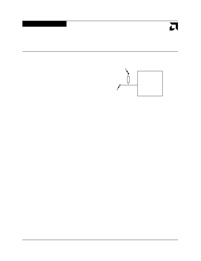
VCO, AMD strongly recommends that the low-pass filter
shown below be implemented on these pins. Tests us-
ing this filter have shown significantly increased noise
immunity and reduced Bit Error Rate (BER) statistics in
designs using the PCnet-ISA controller.
相關(guān)PDF資料 |
PDF描述 |
|---|---|
| AM79C960KC | PCnetTM-ISA Single-Chip Ethernet Controller |
| AM79C960KCW | PCnetTM-ISA Single-Chip Ethernet Controller |
| AM79C961AKCW | PCnet ⑩-ISA II Jumperless, Full Duplex Single-Chip Ethernet Controller for ISA |
| AM79C961AKC | PCnet ⑩-ISA II Jumperless, Full Duplex Single-Chip Ethernet Controller for ISA |
| AM79C961A | PCnet ⑩-ISA II Jumperless, Full Duplex Single-Chip Ethernet Controller for ISA |
相關(guān)代理商/技術(shù)參數(shù) |
參數(shù)描述 |
|---|---|
| AM79C960KC | 制造商:AMD 制造商全稱:Advanced Micro Devices 功能描述:PCnetTM-ISA Single-Chip Ethernet Controller |
| AM79C960KC/W | 制造商:未知廠家 制造商全稱:未知廠家 功能描述:LAN Node Controller |
| AM79C960KCW | 制造商:AMD 制造商全稱:Advanced Micro Devices 功能描述:PCnetTM-ISA Single-Chip Ethernet Controller |
| AM79C961 | 制造商:未知廠家 制造商全稱:未知廠家 功能描述:Am79C961 - PCnet-ISA+ Jumperless Single-Chip Ethernet Controller for ISA |
| AM79C961/AM79C961A | 制造商:未知廠家 制造商全稱:未知廠家 功能描述:Using the Am79C961/Am79C961A (PCnet-ISA+/PCnet-ISA II) Survival Guide? 134KB (PDF) |
發(fā)布緊急采購,3分鐘左右您將得到回復(fù)。