- 您現(xiàn)在的位置:買賣IC網(wǎng) > PDF目錄298975 > CY3950V484-125BBC (Cypress Semiconductor Corp.) CPLDs at FPGA Densities PDF資料下載
參數(shù)資料
| 型號(hào): | CY3950V484-125BBC |
| 廠商: | Cypress Semiconductor Corp. |
| 英文描述: | CPLDs at FPGA Densities |
| 中文描述: | CPLD器件在FPGA的密度 |
| 文件頁數(shù): | 4/86頁 |
| 文件大小: | 1212K |
| 代理商: | CY3950V484-125BBC |
第1頁第2頁第3頁當(dāng)前第4頁第5頁第6頁第7頁第8頁第9頁第10頁第11頁第12頁第13頁第14頁第15頁第16頁第17頁第18頁第19頁第20頁第21頁第22頁第23頁第24頁第25頁第26頁第27頁第28頁第29頁第30頁第31頁第32頁第33頁第34頁第35頁第36頁第37頁第38頁第39頁第40頁第41頁第42頁第43頁第44頁第45頁第46頁第47頁第48頁第49頁第50頁第51頁第52頁第53頁第54頁第55頁第56頁第57頁第58頁第59頁第60頁第61頁第62頁第63頁第64頁第65頁第66頁第67頁第68頁第69頁第70頁第71頁第72頁第73頁第74頁第75頁第76頁第77頁第78頁第79頁第80頁第81頁第82頁第83頁第84頁第85頁第86頁
Delta39K ISR
CPLD Family
Document #: 38-03039 Rev. *H
Page 12 of 86
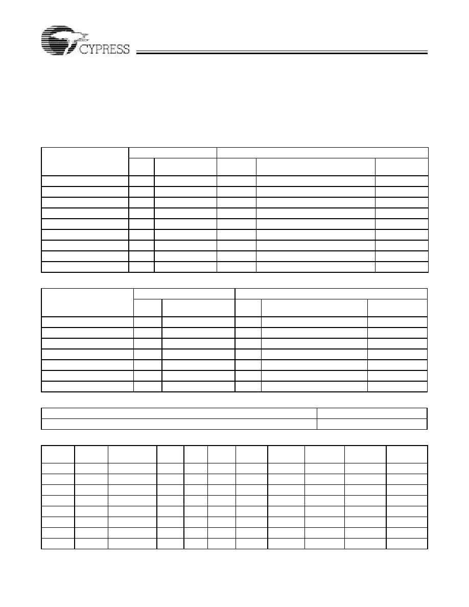
Table 6 describes the valid phase shift options that can be
used with or without an external feedback.
Table 7 is an example of the effect of all the available divide
and phase shift options on a VCO output of 250 MHz. It also
shows the effect of division on the duty cycle of the resultant
clock. Note that the duty cycle is 50-50 when a VCO output is
divided by an even number. Also note that the phase shift
applies to the VCO output and not to the divided output.
For more details on the architecture and operation of this PLL
please refer to the application note entitled “Delta39K PLL and
Clock Tree”.
Table 4. Valid PLL Multiply and Divide Options—without External Feedback
Input Frequency
(GCLK[0])
fPLLI (MHz)
Valid Multiply Options
Valid Divide Options
Value
VCO Output
Frequency (MHz)
Value
Output Frequency (INTCLK[3:0])
fPLLO (MHz)
Off-chip Clock
Frequency
DC–12.5
N/A
DC–12.5
DC–6.25
100–133
1
100–133
1–6, 8, 16
6.25–133
3.125–66
50–133
2
100–266
1–6, 8, 16
6.25–266
3.125–133
33.3–88.7
3
100–266
1–6, 8, 16
6.25–266
3.1–266
25–66
4
100–266
1–6, 8, 16
6.25–266
3.125–133
20–53.2
5
100–266
1–6, 8, 16
6.25–266
3.1–133
16.6–44.3
6
100–266
1–6, 8, 16
6.25–266
3.1–133
12.5–33
8
100–266
1–6, 8, 16
6.25–266
3.125–133
12.5–16.625
16
200–266
1–6, 8, 16
6.25–266
3.125–133
Table 5. Valid PLL Multiply and Divide Options—With External Feedback
Input (GCLK) Frequency
fPLLI (MHz)
Valid Multiply Options
Valid Divide Options
Value
VCO Output
Frequency (MHz)
Value
Output (INTCLK) Frequency
fPLLO (MHz)
Off-chip Clock
Frequency
50–133
1
100–266
1
100–266
50–133
25–66.5
1
100–266
2
50–133
25–66.5
16.67–44.33
1
100–266
3
33.33–88.66
16.67–44.33
12.5–33.25
1
100–266
4
25–66.5
12.5–33.25
12.5–26.6
1
125–266
5
25–53.2
12.5–26.6
12.5–22.17
1
150–266
6
25–44.34
12.5–22.17
12.5–16.63
1
200–266
8
25–33.25
12.5–16.63
Table 6. Recommended PLL Phase Shift Options
Without External Feedback
With External Feedback
0°,45°, 90°, 135°, 180°, 225°, 270°, 315°
0°
Table 7. Timing of Clock Phases for all Divide Options for a VCO Output Frequency of 250 MHz
Divide
Factor
Period
(ns)
Duty Cycle%
0°
(ns)
45°
(ns)
90°
(ns)
135°
(ns)
180°
(ns)
225°
(ns)
270°
(ns)
315°
(ns)
1
4
40–60
0
0.5
1.0
1.5
2.0
2.5
3.0
3.5
2
8
50
0
0.5
1.0
1.5
2.0
2.5
3.0
3.5
3
12
33–67
0
0.5
1.0
1.5
2.0
2.5
3.0
3.5
4
16
50
0
0.5
1.0
1.5
2.0
2.5
3.0
3.5
5
20
40–60
0
0.5
1.0
1.5
2.0
2.5
3.0
3.5
6
24
50
0
0.5
1.0
1.5
2.0
2.5
3.0
3.5
8
32
50
0
0.5
1.0
1.5
2.0
2.5
3.0
3.5
16
64
50
0
0.5
1.0
1.5
2.0
2.5
3.0
3.5
相關(guān)PDF資料 |
PDF描述 |
|---|---|
| CY54FCT540CTDMB | FCT SERIES, 8-BIT DRIVER, INVERTED OUTPUT, CDIP20 |
| CY54FCT543CTDMB | FCT SERIES, 8-BIT REGISTERED TRANSCEIVER, TRUE OUTPUT, CDIP24 |
| CY54FCT543ATDMB | FCT SERIES, 8-BIT REGISTERED TRANSCEIVER, TRUE OUTPUT, CDIP24 |
| CY54FCT543ATLMB | FCT SERIES, 8-BIT REGISTERED TRANSCEIVER, TRUE OUTPUT, CQCC28 |
| CY54FCT543TLMB | FCT SERIES, 8-BIT REGISTERED TRANSCEIVER, TRUE OUTPUT, CQCC28 |
相關(guān)代理商/技術(shù)參數(shù) |
參數(shù)描述 |
|---|---|
| CY3950V484-125BBI | 制造商:CYPRESS 制造商全稱:Cypress Semiconductor 功能描述:CPLDs at FPGA Densities |
| CY3950V484-125BGC | 制造商:CYPRESS 制造商全稱:Cypress Semiconductor 功能描述:CPLDs at FPGA Densities |
| CY3950V484-125BGI | 制造商:CYPRESS 制造商全稱:Cypress Semiconductor 功能描述:CPLDs at FPGA Densities |
| CY3950V484-125MBC | 制造商:CYPRESS 制造商全稱:Cypress Semiconductor 功能描述:CPLDs at FPGA Densities |
| CY3950V484-125MBI | 制造商:CYPRESS 制造商全稱:Cypress Semiconductor 功能描述:CPLDs at FPGA Densities |
發(fā)布緊急采購,3分鐘左右您將得到回復(fù)。