- 您現(xiàn)在的位置:買(mǎi)賣(mài)IC網(wǎng) > PDF目錄298975 > CY3950V484-125BBC (Cypress Semiconductor Corp.) CPLDs at FPGA Densities PDF資料下載
參數(shù)資料
| 型號(hào): | CY3950V484-125BBC |
| 廠商: | Cypress Semiconductor Corp. |
| 英文描述: | CPLDs at FPGA Densities |
| 中文描述: | CPLD器件在FPGA的密度 |
| 文件頁(yè)數(shù): | 78/86頁(yè) |
| 文件大小: | 1212K |
| 代理商: | CY3950V484-125BBC |
第1頁(yè)第2頁(yè)第3頁(yè)第4頁(yè)第5頁(yè)第6頁(yè)第7頁(yè)第8頁(yè)第9頁(yè)第10頁(yè)第11頁(yè)第12頁(yè)第13頁(yè)第14頁(yè)第15頁(yè)第16頁(yè)第17頁(yè)第18頁(yè)第19頁(yè)第20頁(yè)第21頁(yè)第22頁(yè)第23頁(yè)第24頁(yè)第25頁(yè)第26頁(yè)第27頁(yè)第28頁(yè)第29頁(yè)第30頁(yè)第31頁(yè)第32頁(yè)第33頁(yè)第34頁(yè)第35頁(yè)第36頁(yè)第37頁(yè)第38頁(yè)第39頁(yè)第40頁(yè)第41頁(yè)第42頁(yè)第43頁(yè)第44頁(yè)第45頁(yè)第46頁(yè)第47頁(yè)第48頁(yè)第49頁(yè)第50頁(yè)第51頁(yè)第52頁(yè)第53頁(yè)第54頁(yè)第55頁(yè)第56頁(yè)第57頁(yè)第58頁(yè)第59頁(yè)第60頁(yè)第61頁(yè)第62頁(yè)第63頁(yè)第64頁(yè)第65頁(yè)第66頁(yè)第67頁(yè)第68頁(yè)第69頁(yè)第70頁(yè)第71頁(yè)第72頁(yè)第73頁(yè)第74頁(yè)第75頁(yè)第76頁(yè)第77頁(yè)當(dāng)前第78頁(yè)第79頁(yè)第80頁(yè)第81頁(yè)第82頁(yè)第83頁(yè)第84頁(yè)第85頁(yè)第86頁(yè)
Delta39K ISR
CPLD Family
Document #: 38-03039 Rev. *H
Page 8 of 86
The clocks for each port of the Dual-Port configuration are
selected from four global clocks and two local clocks. One
local clock is sourced from the horizontal channel and the
other from the vertical channel. The data outputs of the dual-
port memory can also be registered. Clocks for the output
registers are also selected from four global clocks and two
local clocks. One clock polarity mux per port allows the use of
true or complement polarity for input and output clocking
purposes.
Arbitration
The Dual-Port configuration of the Channel Memory Block
provides arbitration when both ports access the same address
at the same time. Depending on the memory operation being
attempted, one port always gets priority. See Table 2 for
details on which port gets priority for Read and Write opera-
tions. An active-LOW “Address Match” signal is generated
when an address collision occurs.
FIFO (Channel Memory) Configuration
The channel memory blocks are also configurable as
synchronous FIFO RAM. In the FIFO mode of operation, the
channel memory block supports all normal FIFO operations
without the use of any general-purpose logic resources in the
device.
The FIFO block contains all of the necessary FIFO flag logic,
including the Read and Write address pointers. The FIFO flags
include an empty/full flag (EF), half-full flag (HF), and program-
mable almost-empty/full (PAEF) flag output. The FIFO config-
uration has the ability to perform simultaneous Read and Write
operations using two separate clocks. These clocks may be
tied together for a single operation or may run independently
for asynchronous Read/Write (with regard to each other) appli-
cations. The data and control inputs to the FIFO block are
driven from the horizontal or vertical routing channels. The
data and flag outputs are driven onto dedicated routing tracks
in both the horizontal and vertical routing channels. This allows
the FIFO blocks to be expanded by using multiple FIFO blocks
on the same horizontal or vertical routing channel without any
speed penalty.
In FIFO mode, the Write and Read ports are controlled by
separate clock and enable signals. The clocks for each port
are selected from four global clocks and two local clocks.
One local clock is sourced from the horizontal channel and the
other from the vertical channel. The data outputs from the
Read port of the FIFO can also be registered. One clock
polarity mux per port allows using true or complement polarity
for Read and Write operations. The Write operation is
controlled by the clock and the Write enable pin. The Read
operation is controlled by the clock and the Read enable pin.
The enable pins can be sourced from horizontal or vertical
channels.
Channel Memory Initialization
The channel memory powers up in an undefined state, but is
set to a user-defined known state during configuration. To facil-
itate the use of look-up-table (LUT) logic and ROM applica-
tions, the channel memory blocks can be initialized with a
given set of data when the device is configured at power up.
For LUT and ROM applications, the user cannot write to
memory blocks.
Channel Memory Routing Interface
Similar to LBC outputs, the channel memory blocks feature
dedicated tracks in the horizontal and vertical routing channels
for the data outputs and the flag outputs, as shown in
Figure 6. This allows the channel memory blocks to be
expanded easily. These dedicated lines can be routed to I/O
pins as chip outputs or to other logic block clusters to be used
in logic equations.
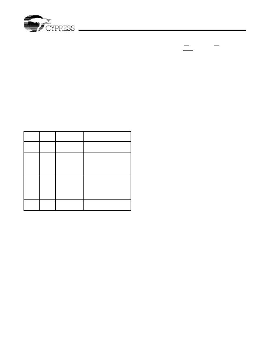
Table 2. Arbitration Result: Address Match Signal
Becomes Active
Port A
Port B
Result of
Arbitration
Comment
Read
No arbitration
required
Both ports read at the
same time
Write
Read
Port A gets
priority
If Port B requests first then
it will read the current
data. The output will then
change to the newly
written data by Port A
Read
Write
Port B gets
priority
If Port A requests first then
it will read the current
data. The output will then
change to the newly
written data by Port B
Write
Port A gets
priority
Port B is blocked until Port
A is finished writing
相關(guān)PDF資料 |
PDF描述 |
|---|---|
| CY54FCT540CTDMB | FCT SERIES, 8-BIT DRIVER, INVERTED OUTPUT, CDIP20 |
| CY54FCT543CTDMB | FCT SERIES, 8-BIT REGISTERED TRANSCEIVER, TRUE OUTPUT, CDIP24 |
| CY54FCT543ATDMB | FCT SERIES, 8-BIT REGISTERED TRANSCEIVER, TRUE OUTPUT, CDIP24 |
| CY54FCT543ATLMB | FCT SERIES, 8-BIT REGISTERED TRANSCEIVER, TRUE OUTPUT, CQCC28 |
| CY54FCT543TLMB | FCT SERIES, 8-BIT REGISTERED TRANSCEIVER, TRUE OUTPUT, CQCC28 |
相關(guān)代理商/技術(shù)參數(shù) |
參數(shù)描述 |
|---|---|
| CY3950V484-125BBI | 制造商:CYPRESS 制造商全稱(chēng):Cypress Semiconductor 功能描述:CPLDs at FPGA Densities |
| CY3950V484-125BGC | 制造商:CYPRESS 制造商全稱(chēng):Cypress Semiconductor 功能描述:CPLDs at FPGA Densities |
| CY3950V484-125BGI | 制造商:CYPRESS 制造商全稱(chēng):Cypress Semiconductor 功能描述:CPLDs at FPGA Densities |
| CY3950V484-125MBC | 制造商:CYPRESS 制造商全稱(chēng):Cypress Semiconductor 功能描述:CPLDs at FPGA Densities |
| CY3950V484-125MBI | 制造商:CYPRESS 制造商全稱(chēng):Cypress Semiconductor 功能描述:CPLDs at FPGA Densities |
發(fā)布緊急采購(gòu),3分鐘左右您將得到回復(fù)。