- 您現(xiàn)在的位置:買賣IC網(wǎng) > PDF目錄384279 > EDD51321CBH (Elpida Memory, Inc.) 512M bits DDR SDRAM PDF資料下載
參數(shù)資料
| 型號: | EDD51321CBH |
| 廠商: | Elpida Memory, Inc. |
| 英文描述: | 512M bits DDR SDRAM |
| 中文描述: | 512M比特DDR內(nèi)存 |
| 文件頁數(shù): | 1/55頁 |
| 文件大?。?/td> | 589K |
| 代理商: | EDD51321CBH |
當前第1頁第2頁第3頁第4頁第5頁第6頁第7頁第8頁第9頁第10頁第11頁第12頁第13頁第14頁第15頁第16頁第17頁第18頁第19頁第20頁第21頁第22頁第23頁第24頁第25頁第26頁第27頁第28頁第29頁第30頁第31頁第32頁第33頁第34頁第35頁第36頁第37頁第38頁第39頁第40頁第41頁第42頁第43頁第44頁第45頁第46頁第47頁第48頁第49頁第50頁第51頁第52頁第53頁第54頁第55頁
Document No. E1094E30 (Ver. 3.0)
Date Published November 2007 (K) Japan
Printed in Japan
URL: http://www.elpida.com
Elpida Memory, Inc. 2007
PRELIMINARY DATA SHEET
512M bits DDR SDRAM
EDD51321CBH (16M words
×
32 bits)
Specifications
Density: 512M bits
Organization
×
32 bits: 4M words
×
32 bits
×
4 banks
Package: 90-ball FBGA
Lead-free (RoHS compliant)
Power supply: VDD, VDDQ
=
1.8V +0.15V/–0.1V
Clock frequency: 166MHz/133MHz (max.)
2KB page size
Row address: A0 to A12
Column address: A0 to A8
Four internal banks for concurrent operation
Interface: LVCMOS
Burst lengths (BL): 2, 4, 8
Burst type (BT):
Sequential (2, 4, 8)
Interleave (2, 4, 8)
/CAS Latency (CL): 3
Precharge: auto precharge option for each burst
access
Driver strength: full/half/quarter
Refresh: auto-refresh, self-refresh
Refresh cycles: 8192 cycles/64ms
Average refresh period: 7.8
μ
s
Operating ambient temperature range
TA =
20
°
C to +85
°
C
Features
DLL is not implemented
Low power consumption
Double-data-rate architecture; two data transfers per
one clock cycle
Bi-directional data strobe (DQS) is transmitted
/received with data for capturing data at the receiver.
DQS is edge-aligned with data for READs; center-
aligned with data for WRITEs
Differential clock inputs (CK and /CK)
Commands entered on each positive CK edge: data
and data mask referenced to both edges of DQS
Burst termination by burst stop command and
Precharge command
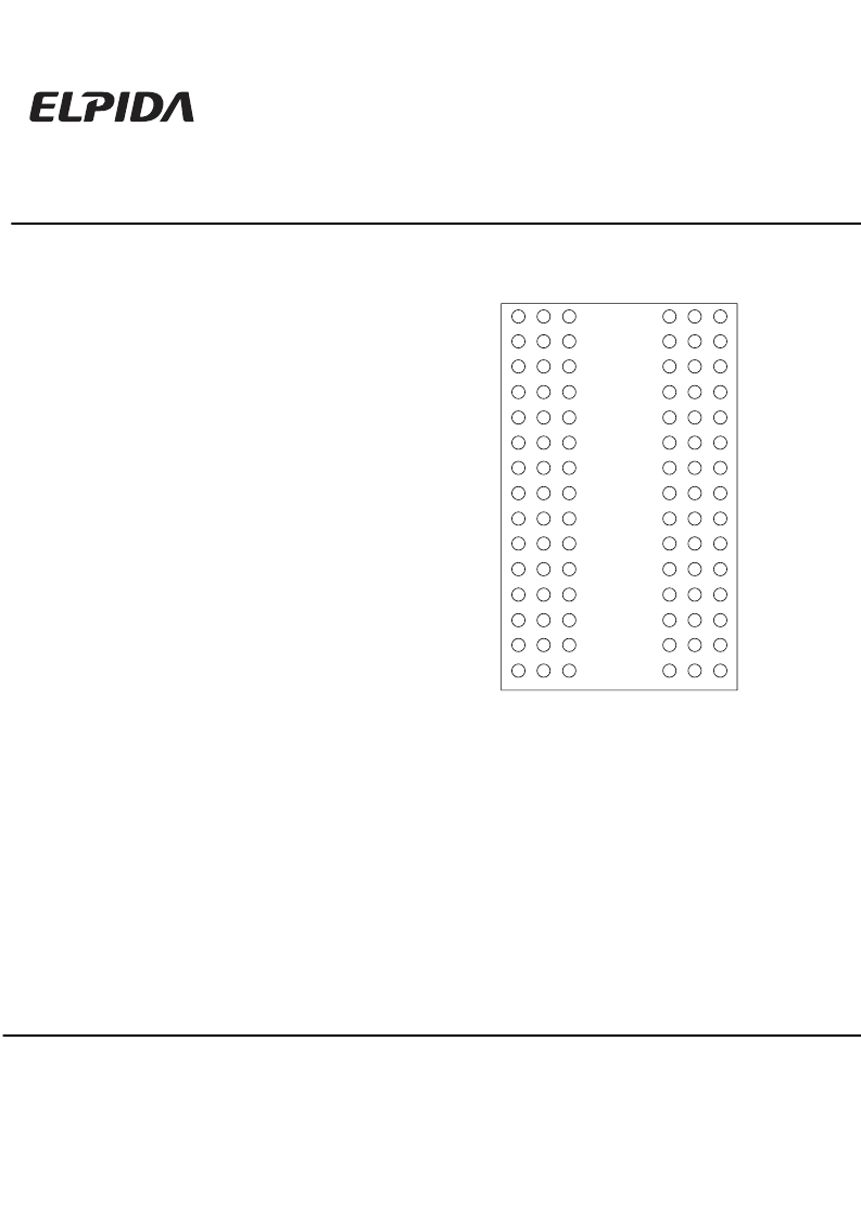
Pin Configurations
/xxx indicate active low signal.
VSS
1
A
B
C
D
E
F
G
H
J
K
L
M
N
P
R
2
3
4
5
6
7
8
9
VDDQ
VSSQ
VDDQ
VSSQ
VDD
CKE
A9
A6
DQ31
DQ29
DQ27
DQ25
DQS3
DM3
CK
A11
A7
VSSQ
DQ30
DQ28
DQ26
DQ24
NC
/CK
A12
A8
VDDQ
DQ17
DQ19
DQ21
DQ23
NC
/WE
/CS
A10 (AP)
DQ16
DQ18
DQ20
DQ22
DQS2
DM2
/CAS
BA0
A0
VDD
VSSQ
VDDQ
VSSQ
VDDQ
VSS
/RAS
BA1
A1
(Top view)
A4
DM1
A5
A2
DM0
A3
VSSQ DQS1 DQ8
DQ7 DQS0 VDDQ
VDDQ DQ9 DQ10
DQ5
DQ6 VSSQ
VSSQ DQ11 DQ12
DQ3
DQ4 VDDQ
VDDQ DQ13 DQ14
DQ1
DQ2 VSSQ
VSS DQ15 VSSQ
VDDQ DQ0
VDD
90-ball FBGA
Address inputs
Bank select address
Data-input/output
Input and output data strobe
Chip select
Row address strobe
Column address strobe
Write enable
Input mask
Clock enable
Clock input
Differential clock input
Power for internal circuit
Ground for internal circuit
Power for DQ circuit
Ground for DQ circuit
No connection
A0 to A12
BA0, BA1
DQ0 to DQ31
DQS0 to DQS3
/CS
/RAS
/CAS
/WE
DM0 to DM3
CKE
CK
/CK
VDD
VSS
VDDQ
VSSQ
NC
相關PDF資料 |
PDF描述 |
|---|---|
| EDD51321CBH-6CTT-E | 512M bits DDR SDRAM |
| EDD51321CBH-7ETT-E | 512M bits DDR SDRAM |
| EDE1116ABSE-6E-E | 1G bits DDR2 SDRAM |
| EDE1104ABSE | 1G bits DDR2 SDRAM |
| EDE1104ABSE-4A-E | 1G bits DDR2 SDRAM |
相關代理商/技術(shù)參數(shù) |
參數(shù)描述 |
|---|---|
| EDD51321CBH-6CTT-E | 制造商:ELPIDA 制造商全稱:Elpida Memory 功能描述:512M bits DDR SDRAM |
| EDD51321CBH-7ETT-E | 制造商:ELPIDA 制造商全稱:Elpida Memory 功能描述:512M bits DDR SDRAM |
| EDD51321DBH-5BTS-F | 制造商:ELPIDA 制造商全稱:Elpida Memory 功能描述:512M bits DDR Mobile RAM? WTR (Wide Temperature Range) |
| EDD51321DBH-6ETS-F | 制造商:ELPIDA 制造商全稱:Elpida Memory 功能描述:512M bits DDR Mobile RAM? WTR (Wide Temperature Range) |
| EDD51321DBH-TS | 制造商:ELPIDA 制造商全稱:Elpida Memory 功能描述:512M bits DDR Mobile RAM? WTR (Wide Temperature Range) |
發(fā)布緊急采購,3分鐘左右您將得到回復。