- 您現(xiàn)在的位置:買賣IC網(wǎng) > PDF目錄375864 > FMS7401 (Fairchild Semiconductor Corporation) Digital Power Controller PDF資料下載
參數(shù)資料
| 型號: | FMS7401 |
| 廠商: | Fairchild Semiconductor Corporation |
| 元件分類: | 基準電壓源/電流源 |
| 英文描述: | Digital Power Controller |
| 中文描述: | 數(shù)字電源控制器 |
| 文件頁數(shù): | 26/80頁 |
| 文件大?。?/td> | 1535K |
| 代理商: | FMS7401 |
第1頁第2頁第3頁第4頁第5頁第6頁第7頁第8頁第9頁第10頁第11頁第12頁第13頁第14頁第15頁第16頁第17頁第18頁第19頁第20頁第21頁第22頁第23頁第24頁第25頁當前第26頁第27頁第28頁第29頁第30頁第31頁第32頁第33頁第34頁第35頁第36頁第37頁第38頁第39頁第40頁第41頁第42頁第43頁第44頁第45頁第46頁第47頁第48頁第49頁第50頁第51頁第52頁第53頁第54頁第55頁第56頁第57頁第58頁第59頁第60頁第61頁第62頁第63頁第64頁第65頁第66頁第67頁第68頁第69頁第70頁第71頁第72頁第73頁第74頁第75頁第76頁第77頁第78頁第79頁第80頁
FMS7401/7401L
PRODUCT SPECIFICATION
26
REV. 1.0.2 6/23/04
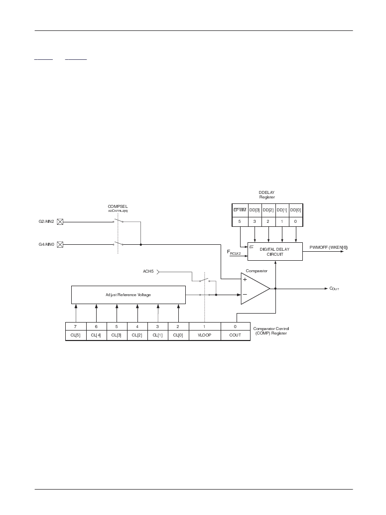
Bits 7-2 (CL[5:0]) is the comparator voltage threshold level selection bits of the Comparator Control (COMP) register. The CL
bits may be programmed to select one of the voltage threshold levels as the inverting input of the analog comparator. Refer to
Table 9
and
Table 10
for a detailed list of voltages.
Bit 1 of the Comparator Control (COMP) register is the Programmable Comparator circuit’s voltage loop (VLOOP) configura-
tion enable bit. If VLOOP=0, the Programmable Comparator circuit is configured to compare the analog G4/AIN0 or G2/AIN2
input (COMPSEL=0 or 1) to one of the 63 voltage threshold levels. If VLOOP=1, enables the voltage loop configuration where
the analog G4/AIN0 or G2/AIN2 input (COMPSEL=0 or 1) to the Uncommitted (Error) Amplifier output (A
OUT
).
Bit 7 of the Digital Delay (DDELAY) register is the Programmable Comparator circuit enable (COMPEN) bit. If COMPEN=0,
the Programmable Comparator circuit is disabled and the C
OUT
signal is low. If COMPEN=1, the Programmable Comparator
circuit is enabled and the C
OUT
signal generated by the comparison of the two inputs.
The comparator output (C
OUT
) signal is latched by the main system instruction (F
ICLK
) clock into bit 0 (COUT) of the Compar-
ator Control (COMP) register. Software may only read the COUT bit to monitor the comparator’s activity. The COUT bit
cannot cause a microcontroller hardware interrupt or perform any other action.
Figure 8. Programmable Comparator Block Diagram (VLOOP = 0)
DDELAY
Register
7
C
L
[5]
1
V
L
OOP
0
C
O
UT
A
d
ju
st
Re
f
ere
nc
e
V
ol
t
a
ge
C
o
mp
a
r
a
t
r
C
tr
ol
(
C
O
M
P
)
Register
G4/
A
IN
0
_
+
D
IGI
T
AL
DELAY
C
I
R
C
U
I
T
3
2
1
0
P
W
M
O
FF
(
WK
E
N
[
6
]
)
DD
[
3
]
DD
[
2
]
DD
[
1
]
DD
[
0
]
F
R
C
L
K
2
5
E
P
W
M
E
n
6
C
L
[
4
]
5
C
L
[
3
]
4
C
L
[
2
]
3
C
L
[
1
]
2
C
L
[
0
]
A
C
H
5
G
2
/
A
IN
2
C
O
M
P
S
EL
AD
C
N
T
R
L
2
[
6
]
C
o
mp
a
r
a
t
o
r
C
O
UT
相關PDF資料 |
PDF描述 |
|---|---|
| FMS7401LEN | Digital Power Controller |
| FMS7401LEN14 | Digital Power Controller |
| FMS7401LVN | Digital Power Controller |
| FMS7401LVN14 | Digital Power Controller |
| FMS7G10US60S | SWTCH ROLLER SPDT 20A SCRW TERM |
相關代理商/技術參數(shù) |
參數(shù)描述 |
|---|---|
| FMS7401L | 制造商:FAIRCHILD 制造商全稱:Fairchild Semiconductor 功能描述:Digital Power Controller |
| FMS7401L_05 | 制造商:FAIRCHILD 制造商全稱:Fairchild Semiconductor 功能描述:Digital Power Controller |
| FMS7401LA_ABA3026U WAF | 制造商:Fairchild Semiconductor Corporation 功能描述: |
| FMS7401LEM8X | 制造商:FAIRCHILD 制造商全稱:Fairchild Semiconductor 功能描述:Digital Power Controller |
| FMS7401LEMT8X | 制造商:FAIRCHILD 制造商全稱:Fairchild Semiconductor 功能描述:Digital Power Controller |
發(fā)布緊急采購,3分鐘左右您將得到回復。