- 您現(xiàn)在的位置:買(mǎi)賣(mài)IC網(wǎng) > PDF目錄375864 > FMS7401 (Fairchild Semiconductor Corporation) Digital Power Controller PDF資料下載
參數(shù)資料
| 型號(hào): | FMS7401 |
| 廠商: | Fairchild Semiconductor Corporation |
| 元件分類(lèi): | 基準(zhǔn)電壓源/電流源 |
| 英文描述: | Digital Power Controller |
| 中文描述: | 數(shù)字電源控制器 |
| 文件頁(yè)數(shù): | 40/80頁(yè) |
| 文件大小: | 1535K |
| 代理商: | FMS7401 |
第1頁(yè)第2頁(yè)第3頁(yè)第4頁(yè)第5頁(yè)第6頁(yè)第7頁(yè)第8頁(yè)第9頁(yè)第10頁(yè)第11頁(yè)第12頁(yè)第13頁(yè)第14頁(yè)第15頁(yè)第16頁(yè)第17頁(yè)第18頁(yè)第19頁(yè)第20頁(yè)第21頁(yè)第22頁(yè)第23頁(yè)第24頁(yè)第25頁(yè)第26頁(yè)第27頁(yè)第28頁(yè)第29頁(yè)第30頁(yè)第31頁(yè)第32頁(yè)第33頁(yè)第34頁(yè)第35頁(yè)第36頁(yè)第37頁(yè)第38頁(yè)第39頁(yè)當(dāng)前第40頁(yè)第41頁(yè)第42頁(yè)第43頁(yè)第44頁(yè)第45頁(yè)第46頁(yè)第47頁(yè)第48頁(yè)第49頁(yè)第50頁(yè)第51頁(yè)第52頁(yè)第53頁(yè)第54頁(yè)第55頁(yè)第56頁(yè)第57頁(yè)第58頁(yè)第59頁(yè)第60頁(yè)第61頁(yè)第62頁(yè)第63頁(yè)第64頁(yè)第65頁(yè)第66頁(yè)第67頁(yè)第68頁(yè)第69頁(yè)第70頁(yè)第71頁(yè)第72頁(yè)第73頁(yè)第74頁(yè)第75頁(yè)第76頁(yè)第77頁(yè)第78頁(yè)第79頁(yè)第80頁(yè)

FMS7401/7401L
PRODUCT SPECIFICATION
40
REV. 1.0.2 6/23/04
6.3
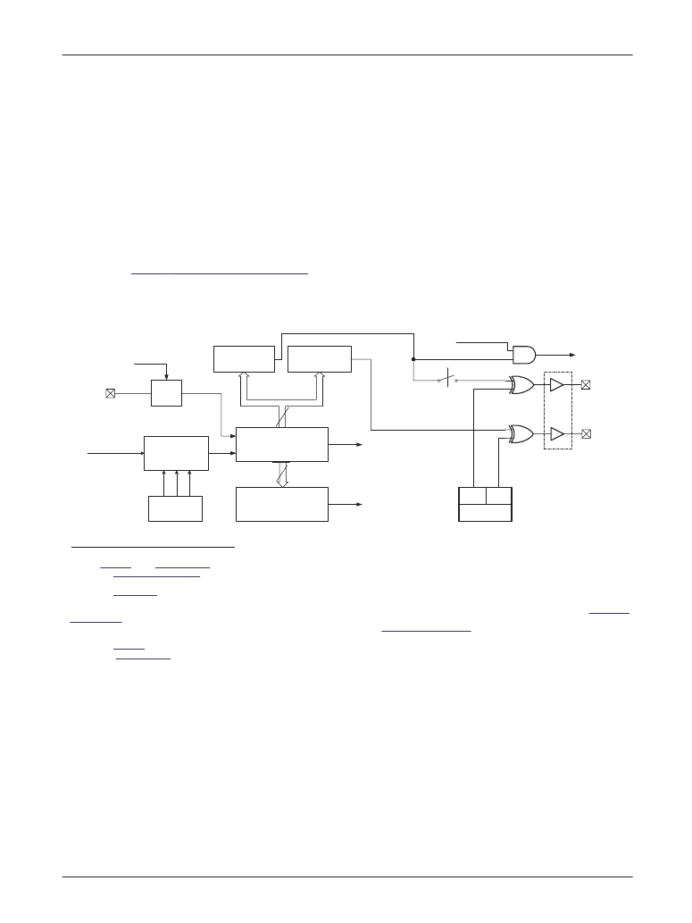
When the PWM Timer 1 circuit is configured in Input Capture Mode, the T1HS2 signal is used as an input of the Timer 1
circuit instead of an output as in PWM Mode. The G5/T1HS2 device pin should be configured by software as an input port.
The Timer 1 circuit may be programmed to capture the TMR1 counter value in the T1RA register with every rising or falling
edge transition of the T1HS2 input. With each TMR1 capture, the T1PND bit of the T1CNTRL register is set. For synchroniza-
tion purposes, the T1HS2 input is synchronized with the F
T1CLK
clock before being allowed to trigger a TMR1 capture. A max-
imum of three F
T1CLK
cycle TMR1 capture delay will occur with each edge transition on the G5/T1HS2 device pin.
Input Capture Mode
Once the Timer 1 circuit is configured for Input Capture Mode, the TMR1 counter starts incrementing continuously from
0x000 through 0xFFF until the Timer 1 is returned to a disabled PWM operating mode. Once the TMR1 counter overflows
(transitions from 0xFFF to 0x000) the T1C0 pending bit on through T1CNTRL register is set.
In Input Capture Mode, it is still possible to generate output signals with variable duty-cycle thanks to the T1CMPA and
T1CMPB compare registers. If enabled, the T1HS1 and ADSTROBE output signals may be generated as in PWM Mode. Refer
to the previous
Pulse Width Modulation (PWM) Mode
section of the datasheet for details.
Figure 13. Timer 1’s Input Capture Mode Block Diagram
1. Refer to
Table 30
of the
Device Memory
section of the datasheet for the detailed memory map.
2. Refer to the
Electrical Characteristics
section of the datasheet.
3. The PLL’s (F
(FS=0)
) output is not affected by the FS[1:0] bit value of the PSCALE register and merely shares the FS[1:0]=00 divide factor.
4. Refer to the
ADC Circuit
section of the datasheet for additional details.
5. The three PS bits have no affect on the dead time, only the TMR1 counter.
6. Hardware interrupts are not executed by the microcontroller core unless the Global Interrupt enable (G) flag of the Status register is set. Refer to the
8-Bit Micro-
controller Core
section of the datasheet for details.
7. The Timer 1 hardware interrupt will be executed in the defined priority order. Refer to the
8-Bit Microcontroller Core
section of the datasheet for details.
8. The full bridge requires two additional output ports to complete the bridge configuration.
9. Refer to the
I/O Ports
section of the datasheet for additional details.
10.Refer to the
Device Memory
section of the datasheet for details regarding the initialization registers.
T1RA
TMR1
PORTGD
G0/T1HS1
F
T1CLK
12
CLOCK
DIVIDER
PS2 PS1 PS0
PSCALE
[11:0]
1
T1CMPA
[11:0]
TMR1=T1CMPB
ENDAS
ADSTROBE
12
G1/AIN3
0
T1CMPB
[11:0]
TMR1=T1CMPA
T1C0
Edge
Control
T1C2
T1PND
Fin
Fout
[11:0]
T1BOUT
G5/T1HS2
相關(guān)PDF資料 |
PDF描述 |
|---|---|
| FMS7401LEN | Digital Power Controller |
| FMS7401LEN14 | Digital Power Controller |
| FMS7401LVN | Digital Power Controller |
| FMS7401LVN14 | Digital Power Controller |
| FMS7G10US60S | SWTCH ROLLER SPDT 20A SCRW TERM |
相關(guān)代理商/技術(shù)參數(shù) |
參數(shù)描述 |
|---|---|
| FMS7401L | 制造商:FAIRCHILD 制造商全稱(chēng):Fairchild Semiconductor 功能描述:Digital Power Controller |
| FMS7401L_05 | 制造商:FAIRCHILD 制造商全稱(chēng):Fairchild Semiconductor 功能描述:Digital Power Controller |
| FMS7401LA_ABA3026U WAF | 制造商:Fairchild Semiconductor Corporation 功能描述: |
| FMS7401LEM8X | 制造商:FAIRCHILD 制造商全稱(chēng):Fairchild Semiconductor 功能描述:Digital Power Controller |
| FMS7401LEMT8X | 制造商:FAIRCHILD 制造商全稱(chēng):Fairchild Semiconductor 功能描述:Digital Power Controller |
發(fā)布緊急采購(gòu),3分鐘左右您將得到回復(fù)。