- 您現(xiàn)在的位置:買(mǎi)賣(mài)IC網(wǎng) > PDF目錄224505 > MT46V32M16TG-75ELIT 32M X 16 DDR DRAM, 0.75 ns, PDSO66 PDF資料下載
參數(shù)資料
| 型號(hào): | MT46V32M16TG-75ELIT |
| 元件分類(lèi): | DRAM |
| 英文描述: | 32M X 16 DDR DRAM, 0.75 ns, PDSO66 |
| 封裝: | 0.400 INCH, PLASTIC, TSOP-66 |
| 文件頁(yè)數(shù): | 60/82頁(yè) |
| 文件大?。?/td> | 2855K |
| 代理商: | MT46V32M16TG-75ELIT |
第1頁(yè)第2頁(yè)第3頁(yè)第4頁(yè)第5頁(yè)第6頁(yè)第7頁(yè)第8頁(yè)第9頁(yè)第10頁(yè)第11頁(yè)第12頁(yè)第13頁(yè)第14頁(yè)第15頁(yè)第16頁(yè)第17頁(yè)第18頁(yè)第19頁(yè)第20頁(yè)第21頁(yè)第22頁(yè)第23頁(yè)第24頁(yè)第25頁(yè)第26頁(yè)第27頁(yè)第28頁(yè)第29頁(yè)第30頁(yè)第31頁(yè)第32頁(yè)第33頁(yè)第34頁(yè)第35頁(yè)第36頁(yè)第37頁(yè)第38頁(yè)第39頁(yè)第40頁(yè)第41頁(yè)第42頁(yè)第43頁(yè)第44頁(yè)第45頁(yè)第46頁(yè)第47頁(yè)第48頁(yè)第49頁(yè)第50頁(yè)第51頁(yè)第52頁(yè)第53頁(yè)第54頁(yè)第55頁(yè)第56頁(yè)第57頁(yè)第58頁(yè)第59頁(yè)當(dāng)前第60頁(yè)第61頁(yè)第62頁(yè)第63頁(yè)第64頁(yè)第65頁(yè)第66頁(yè)第67頁(yè)第68頁(yè)第69頁(yè)第70頁(yè)第71頁(yè)第72頁(yè)第73頁(yè)第74頁(yè)第75頁(yè)第76頁(yè)第77頁(yè)第78頁(yè)第79頁(yè)第80頁(yè)第81頁(yè)第82頁(yè)
512Mb: x4, x8, x16
DDR SDRAM
09005aef80a1d9e7
Micron Technology, Inc., reserves the right to change products or specifications without notice.
512MBDDRx4x8x16_2.fm - Rev. H 7/04 EN
63
2000 Micron Technology, Inc. All rights reserved.
31. DQ and DM input slew rates must not deviate
from DQS by more than 10 percent. If the DQ/
DM/DQS slew rate is less than 0.5V/ns, timing
must be derated: 50ps must be added to tDS and
tDH for each 100mv/ns reduction in slew rate. For
-5B, -6 and -6T speed grades, slew rate must be
≥ 0.5V/ns. If slew rate exceeds 4V/ns, functionality
is uncertain.
32. VDD must not vary more than 4 percent if CKE is
not active while any bank is active.
33. The clock is allowed up to ±150ps of jitter. Each
timing parameter is allowed to vary by the same
amount.
34. tHP (MIN) is the lesser of tCL minimum and tCH
minimum actually applied to the device CK and
CK# inputs, collectively during bank active.
35. READs and WRITEs with auto precharge are not
allowed to be issued until tRAS (MIN) can be satis-
fied prior to the internal precharge command
being issued.
36. Any positive glitch must be less than 1/3 of the
clock cycle and not more than +400mV or 2.9V
(+300mV or 2.9V maximum for -5B), whichever is
less. Any negative glitch must be less than 1/3 of
the clock cycle and not exceed either -300mV or
2.2V (2.4V for -5B), whichever is more positive.
The average cannot be below the +2.5V (2.6V for
-5B) minimum.
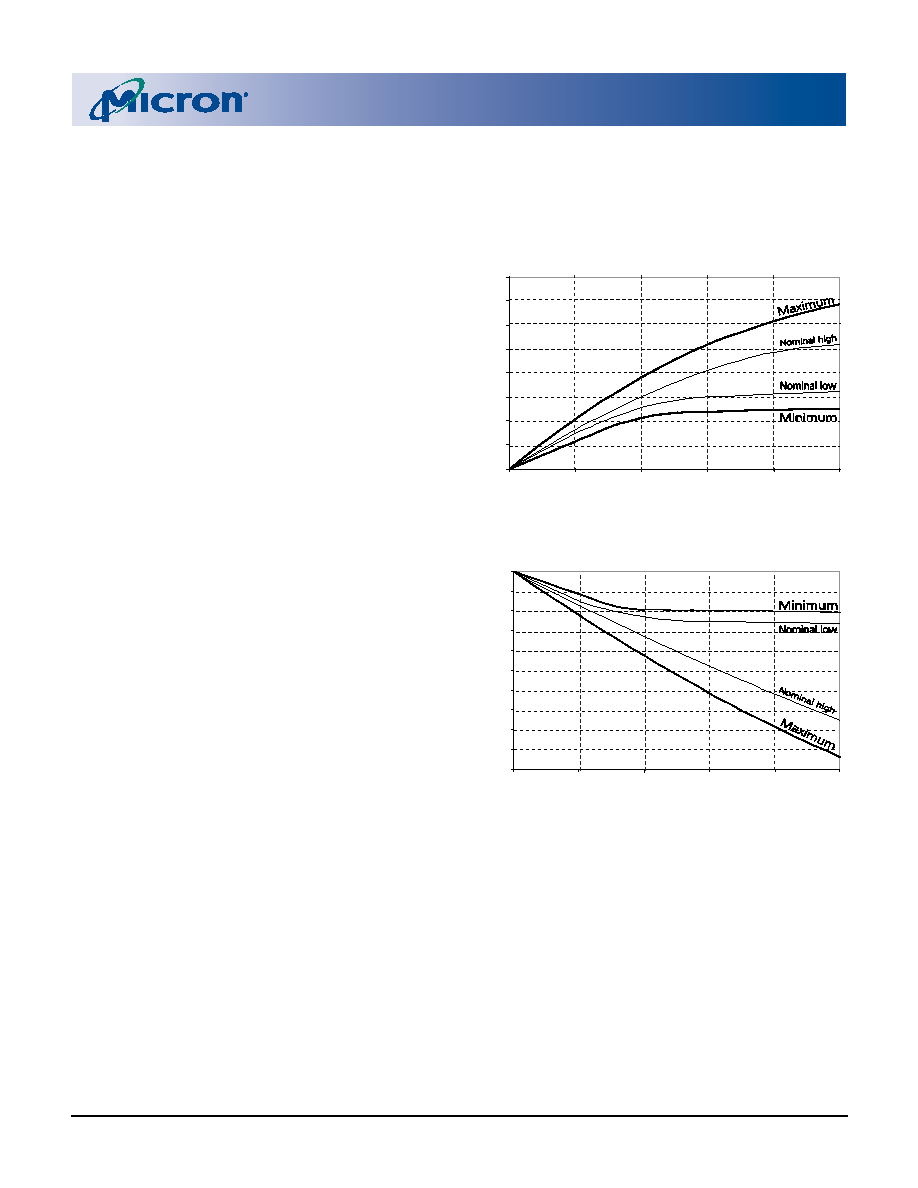
37. Normal Output Drive Curves:
a. The full variation in driver pull-down current
from minimum to maximum process, temper-
ature and voltage will lie within the outer
bounding lines of the V-I curve of Figure 36
b. The variation in driver pull-down current
within nominal limits of voltage and tempera-
ture is expected, but not guaranteed, to lie
within the inner bounding lines of the V-I
curve of Figure 36.
c. The full variation in driver pull-up current
from minimum to maximum process, temper-
ature and voltage will lie within the outer
bounding lines of the V-I curve of Figure 37.
d. The variation in driver pull-up current within
nominal limits of voltage and temperature is
expected, but not guaranteed, to lie within the
inner bounding lines of the V-I curve of
e. The full variation in the ratio of the maximum
to minimum pull-up and pull-down current
should be between 0.71 and 1.4, for device
drain-to-source voltages from 0.1V to 1.0V, and
at the same voltage and temperature.
f. f ) The full variation in the ratio of the nominal
pull-up to pull-down current should be unity
±10 percent, for device drain-to-source volt-
ages from 0.1V to 1.0V.
Figure 36: Full Drive Pull-Down
Characteristics
Figure 37: Full Drive Pull-Up
Characteristics
38. Reduced Output Drive Curves:
a. The full variation in driver pull-down current
from minimum to maximum process, temper-
ature and voltage will lie within the outer
bounding lines of the V-I curve of Figure 38.
b. The variation in driver pull-down current
within nominal limits of voltage and tempera-
ture is expected, but not guaranteed, to lie
within the inner bounding lines of the V-I
curve of Figure 38.
c. The full variation in driver pull-up current
from minimum to maximum process, temper-
ature and voltage will lie within the outer
bounding lines of the V-I curve of Figure 39.
0
20
40
60
80
100
120
140
160
0.0
0.5
1.0
1.5
2.0
2.5
VOUT (V)
IOUT
(m
A
)
-200
-180
-160
-140
-120
-100
-80
-60
-40
-20
0
0.0
0.5
1.0
1.5
2.0
2.5
VDDQ - V OUT (V )
IOUT
(m
A
)
相關(guān)PDF資料 |
PDF描述 |
|---|---|
| MT46V32M16BN-5BLIT | 32M X 16 DDR DRAM, 0.7 ns, PBGA60 |
| MT46V32M81AZ4-6T:G | 32M X 4 DDR DRAM, 0.75 ns, PDSO66 |
| MT47H128M8HV-187ELIT:E | 128M X 8 DDR DRAM, 0.35 ns, PBGA60 |
| MT47H128M8HQ-187ELAT:E | 128M X 8 DDR DRAM, 0.35 ns, PBGA60 |
| MT48LC2M32B1TG-7 | 2M X 32 SYNCHRONOUS DRAM, 5.5 ns, PDSO86 |
相關(guān)代理商/技術(shù)參數(shù) |
參數(shù)描述 |
|---|---|
| MT46V32M16TG-75L | 制造商:MICRON 制造商全稱(chēng):Micron Technology 功能描述:DOUBLE DATA RATE DDR SDRAM |
| MT46V32M16TG-75Z | 制造商:MICRON 制造商全稱(chēng):Micron Technology 功能描述:DOUBLE DATA RATE DDR SDRAM |
| MT46V32M16TG-75ZL | 制造商:MICRON 制造商全稱(chēng):Micron Technology 功能描述:DOUBLE DATA RATE DDR SDRAM |
發(fā)布緊急采購(gòu),3分鐘左右您將得到回復(fù)。