- 您現(xiàn)在的位置:買賣IC網(wǎng) > PDF目錄11733 > ORSO42G5-3BMN484C (Lattice Semiconductor Corporation)IC TRANCEIVERS FPSC 680FPGAM PDF資料下載
參數(shù)資料
| 型號(hào): | ORSO42G5-3BMN484C |
| 廠商: | Lattice Semiconductor Corporation |
| 文件頁(yè)數(shù): | 104/153頁(yè) |
| 文件大小: | 0K |
| 描述: | IC TRANCEIVERS FPSC 680FPGAM |
| 產(chǎn)品變化通告: | Product Discontinuation 01/Aug/2011 |
| 標(biāo)準(zhǔn)包裝: | 60 |
| 系列: | * |
第1頁(yè)第2頁(yè)第3頁(yè)第4頁(yè)第5頁(yè)第6頁(yè)第7頁(yè)第8頁(yè)第9頁(yè)第10頁(yè)第11頁(yè)第12頁(yè)第13頁(yè)第14頁(yè)第15頁(yè)第16頁(yè)第17頁(yè)第18頁(yè)第19頁(yè)第20頁(yè)第21頁(yè)第22頁(yè)第23頁(yè)第24頁(yè)第25頁(yè)第26頁(yè)第27頁(yè)第28頁(yè)第29頁(yè)第30頁(yè)第31頁(yè)第32頁(yè)第33頁(yè)第34頁(yè)第35頁(yè)第36頁(yè)第37頁(yè)第38頁(yè)第39頁(yè)第40頁(yè)第41頁(yè)第42頁(yè)第43頁(yè)第44頁(yè)第45頁(yè)第46頁(yè)第47頁(yè)第48頁(yè)第49頁(yè)第50頁(yè)第51頁(yè)第52頁(yè)第53頁(yè)第54頁(yè)第55頁(yè)第56頁(yè)第57頁(yè)第58頁(yè)第59頁(yè)第60頁(yè)第61頁(yè)第62頁(yè)第63頁(yè)第64頁(yè)第65頁(yè)第66頁(yè)第67頁(yè)第68頁(yè)第69頁(yè)第70頁(yè)第71頁(yè)第72頁(yè)第73頁(yè)第74頁(yè)第75頁(yè)第76頁(yè)第77頁(yè)第78頁(yè)第79頁(yè)第80頁(yè)第81頁(yè)第82頁(yè)第83頁(yè)第84頁(yè)第85頁(yè)第86頁(yè)第87頁(yè)第88頁(yè)第89頁(yè)第90頁(yè)第91頁(yè)第92頁(yè)第93頁(yè)第94頁(yè)第95頁(yè)第96頁(yè)第97頁(yè)第98頁(yè)第99頁(yè)第100頁(yè)第101頁(yè)第102頁(yè)第103頁(yè)當(dāng)前第104頁(yè)第105頁(yè)第106頁(yè)第107頁(yè)第108頁(yè)第109頁(yè)第110頁(yè)第111頁(yè)第112頁(yè)第113頁(yè)第114頁(yè)第115頁(yè)第116頁(yè)第117頁(yè)第118頁(yè)第119頁(yè)第120頁(yè)第121頁(yè)第122頁(yè)第123頁(yè)第124頁(yè)第125頁(yè)第126頁(yè)第127頁(yè)第128頁(yè)第129頁(yè)第130頁(yè)第131頁(yè)第132頁(yè)第133頁(yè)第134頁(yè)第135頁(yè)第136頁(yè)第137頁(yè)第138頁(yè)第139頁(yè)第140頁(yè)第141頁(yè)第142頁(yè)第143頁(yè)第144頁(yè)第145頁(yè)第146頁(yè)第147頁(yè)第148頁(yè)第149頁(yè)第150頁(yè)第151頁(yè)第152頁(yè)第153頁(yè)
Lattice Semiconductor
ORCA ORSO42G5 and ORSO82G5 Data Sheet
54
There are N x 3 (N = 48) bytes of TOH per row and there are a total of 9 rows in a SONET frame. In cell mode, the
rest of the bytes in each row after the TOH bytes are lled by cells. The rst byte in a cell is a Link Header (LH) byte.
At the end of each frame, there are pad bytes if required.
An important function of the payload block is the grouping of bytes together to be presented to the scramble logic.
Due to the insertion of the LH byte in each cell, the total cell data are not divisible by 4 (4 bytes are sent per 77.76
MHz clock cycle). At the end of each row within a SONET frame, the payload block stops sending cell data and
indicates to the TOH block to insert the next row’s TOH bytes. At the end of the TOH byte transmission, the cell data
transmission is resumed.
At the end of a cell, the cell’s BIP-8 byte is inserted. The next cell’s Link Header byte (LH) immediately follows the
previous cell’s BIP-8 byte. The MSB of the LH byte is the link idle cell indicator bit. The payload block gets this bit
from the MSB of the rst word of a cell in the memory and inserts it into the LH byte for the appropriate cell. The
rest of the LH byte is the link sequence number. This number is incremented for each subsequent cell.
After all cells have been transmitted, the appropriate number of pad bytes are sent. At a link speed of 2.5 GHz,
there are 38,880 bytes (SPE + TOH) per frame. There are 1296 bytes of TOH and 37,584 bytes of SPE. For cell
data of 85 bytes this translates to 442 cells per frame and 14 pad bytes (# of cells per frame = # of bytes of SPE/#
of bytes in a cell).
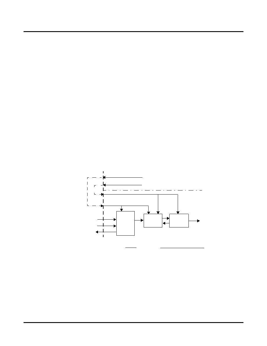
Cell Mode Transmit Timing
Figure 40 shows the transmit clocks and recommended clocking scheme in cell mode. TCK156A, TCK157B can be
used as a 156 MHz clock source for SYSCLK156[A1, A2] and SYSCLK156[B1, B2] respectively. SYSCLK156[A1,
A2] and SYSCLK[B1, B2] are shared with the receive logic in cell mode.
Figure 40. Cell Mode Transmit Timing
When operating in the two-link CELL MODE, each OPC2 Block passes cells from FPGA to embedded core.
Depending upon the congured CELL SIZE, cell transfers will take a variable number of SYSCLK156 cycles to be
transmitted across the interface. Data are always transferred across a 40-bit bus (5 octets per clock cycle).
Figure 41 shows 16 clock cycles for a cell transfer this corresponds to a cell size of 79 octets. The two control sig-
nals in the gure are dened as:
cell_begin_ok: cell request signal from core to FPGA. It will be asserted every 20 or 16 clock cycles (depending
on cell size) when the core is ready to accept cells from FPGA.
OPC2
Payload
TXFIFO
FPGA
Cell Data
TCK78A
SYSCLK156[A:B][1:2]
Cell Valid
Backpressure Signal
TCK156A
or SYSCLK568
Block
TSYSCLKxx
Logic Common to Each Block
Cell Data
Cell Valid
Backpressure Signal
SDO_BP_8
OPC8_CELLVALID
OPC2_[A:B][1:2][39:0]
CELL_BEGIN_OK_[A:B][1:2]
OPC8 [159:0]
OPC2_[A:B][1:2]_CELLVALID
OPC2
OPC8 (ORSO82G5 only)
or
OPC8
(ORSO82G5
only)
相關(guān)PDF資料 |
PDF描述 |
|---|---|
| ORT82G5-1FN680I | IC TRANCEIVERS FPSC 680FPBGA |
| ORT82G5-2FN680I | IC TRANCEIVERS FPSC 680FPBGA |
| VI-J4H-IW-F4 | CONVERTER MOD DC/DC 52V 100W |
| VI-J4H-IW-F3 | CONVERTER MOD DC/DC 52V 100W |
| ORT82G5-1FN680C | IC TRANCEIVERS FPSC 680FPBGA |
相關(guān)代理商/技術(shù)參數(shù) |
參數(shù)描述 |
|---|---|
| ORSO42G5-EV | 功能描述:可編程邏輯 IC 開發(fā)工具 Eval Brd ORSO42G5 RoHS:否 制造商:Altera Corporation 產(chǎn)品:Development Kits 類型:FPGA 工具用于評(píng)估:5CEFA7F3 接口類型: 工作電源電壓: |
| ORSO82G5 | 制造商:LATTICE 制造商全稱:Lattice Semiconductor 功能描述:0.6 to 2.7 Gbps SONET Backplane Interface FPSCs |
| ORSO82G5-1BM680C | 功能描述:FPGA - 現(xiàn)場(chǎng)可編程門陣列 10368 LUT 372 I/O RoHS:否 制造商:Altera Corporation 系列:Cyclone V E 柵極數(shù)量: 邏輯塊數(shù)量:943 內(nèi)嵌式塊RAM - EBR:1956 kbit 輸入/輸出端數(shù)量:128 最大工作頻率:800 MHz 工作電源電壓:1.1 V 最大工作溫度:+ 70 C 安裝風(fēng)格:SMD/SMT 封裝 / 箱體:FBGA-256 |
| ORSO82G5-1BM680I | 功能描述:FPGA - 現(xiàn)場(chǎng)可編程門陣列 10368 LUT 372 I/O RoHS:否 制造商:Altera Corporation 系列:Cyclone V E 柵極數(shù)量: 邏輯塊數(shù)量:943 內(nèi)嵌式塊RAM - EBR:1956 kbit 輸入/輸出端數(shù)量:128 最大工作頻率:800 MHz 工作電源電壓:1.1 V 最大工作溫度:+ 70 C 安裝風(fēng)格:SMD/SMT 封裝 / 箱體:FBGA-256 |
| ORSO82G5-1F680C | 功能描述:FPGA - 現(xiàn)場(chǎng)可編程門陣列 ORCA FPSC 2.7GBITS/s BP XCVR 643K RoHS:否 制造商:Altera Corporation 系列:Cyclone V E 柵極數(shù)量: 邏輯塊數(shù)量:943 內(nèi)嵌式塊RAM - EBR:1956 kbit 輸入/輸出端數(shù)量:128 最大工作頻率:800 MHz 工作電源電壓:1.1 V 最大工作溫度:+ 70 C 安裝風(fēng)格:SMD/SMT 封裝 / 箱體:FBGA-256 |
發(fā)布緊急采購(gòu),3分鐘左右您將得到回復(fù)。