- 您現(xiàn)在的位置:買賣IC網(wǎng) > PDF目錄224693 > PC87393F-VJG (NATIONAL SEMICONDUCTOR CORP) 100-Pin LPC SuperI/O Devices for Portable Applications PDF資料下載
參數(shù)資料
| 型號: | PC87393F-VJG |
| 廠商: | NATIONAL SEMICONDUCTOR CORP |
| 元件分類: | 外設及接口 |
| 英文描述: | 100-Pin LPC SuperI/O Devices for Portable Applications |
| 中文描述: | MULTIFUNCTION PERIPHERAL, PQFP100 |
| 封裝: | TQFP-100 |
| 文件頁數(shù): | 111/148頁 |
| 文件大小: | 1733K |
| 代理商: | PC87393F-VJG |
第1頁第2頁第3頁第4頁第5頁第6頁第7頁第8頁第9頁第10頁第11頁第12頁第13頁第14頁第15頁第16頁第17頁第18頁第19頁第20頁第21頁第22頁第23頁第24頁第25頁第26頁第27頁第28頁第29頁第30頁第31頁第32頁第33頁第34頁第35頁第36頁第37頁第38頁第39頁第40頁第41頁第42頁第43頁第44頁第45頁第46頁第47頁第48頁第49頁第50頁第51頁第52頁第53頁第54頁第55頁第56頁第57頁第58頁第59頁第60頁第61頁第62頁第63頁第64頁第65頁第66頁第67頁第68頁第69頁第70頁第71頁第72頁第73頁第74頁第75頁第76頁第77頁第78頁第79頁第80頁第81頁第82頁第83頁第84頁第85頁第86頁第87頁第88頁第89頁第90頁第91頁第92頁第93頁第94頁第95頁第96頁第97頁第98頁第99頁第100頁第101頁第102頁第103頁第104頁第105頁第106頁第107頁第108頁第109頁第110頁當前第111頁第112頁第113頁第114頁第115頁第116頁第117頁第118頁第119頁第120頁第121頁第122頁第123頁第124頁第125頁第126頁第127頁第128頁第129頁第130頁第131頁第132頁第133頁第134頁第135頁第136頁第137頁第138頁第139頁第140頁第141頁第142頁第143頁第144頁第145頁第146頁第147頁第148頁
2.0 Device Architecture and Configuration (Continued)
65
www.national.com
2.19 X-BUS CONFIGURATION
This section applies to the PC87393 and PC87393F only. FWH-related descriptions apply to the PC87393F only.
2.19.1
Logical Device 15 (X-Bus) Configuration
Table 28 lists the configuration registers that affect the X-Bus functional block. The X-Bus base address registers point to
the X-Bus registers described in the X-Bus chapter. The memory space to which the X-Bus responds is defined by the con-
figuration registers in the following sections. See Sections 2.2.3 and 2.2.4 for a detailed description of the others.
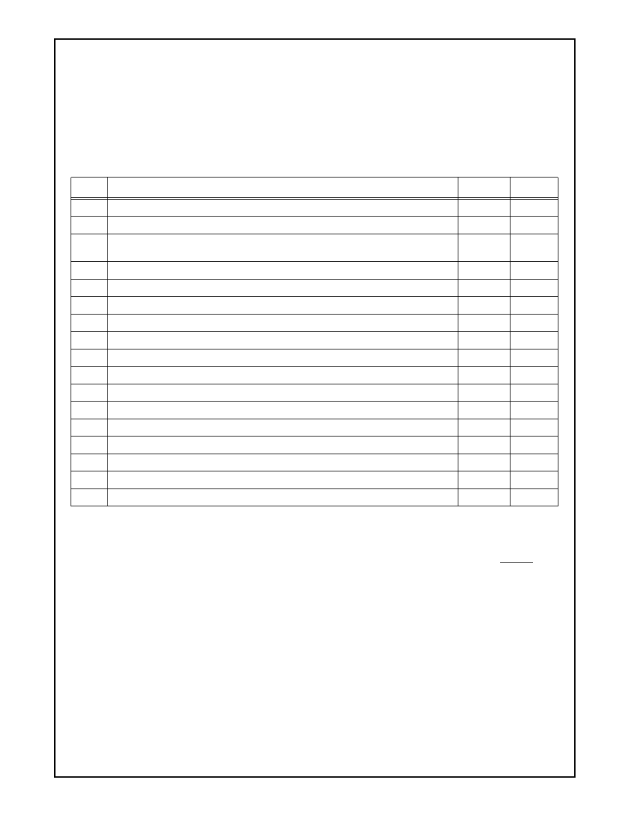
Table 28. X-Bus Conguration Registers
2.19.2
X-Bus I/O Range Programming
LPC I/O transactions can be forwarded to the PC8739x X-Bus. The X-Bus I/O configuration registers define the map of ad-
dresses to be forwarded. The PC8739x provides five, individually enabled I/O zones. Each zone generates an internal select
signal that is sent to the X-Bus functional block. The mapping of the internal select signals to the PC8739x XCS0-1 signals
is controlled by the X-Bus. See Section 7.3 for further details.
The supported I/O zones are:
q
Keyboard controller (KBC) - legacy 60h, 64h addresses and an alternate location
q
Power Management & Embedded Controller (PM) - legacy 62h, 66h and an alternate location
q
Real Time Clock (RTC) - legacy 70h, 71h and two alternate locations
q
User-Dened I/O Zone (UDIZ) - specied using the zone size (2n where n is 1 through 8) and start address (must be
aligned with the block size)
q
Debug Port Address Enable (TST) - This zone is for debug use only.
These decoded I/O zones are determined by the following four registers: X-Bus I/O Configuration, X-Bus I/O Zone Base
Address High and Low Byte, and X-Bus I/O Size Configuration. When a zone (e.g. KBC, PM or RTC) is enabled but is not
associated with any select signal in the X-Bus interface, a value of 00h is read and data written is ignored.
Index
Conguration Register or Action
Type
Reset
30h
Activate. When bit 0 is cleared, the registers of this logical device are not accessible.
R/W
00h
60h
Base Address MSB register
R/W
00h
61h
Base Address LSB register. Bits 3-0 (for A3-A0) are read only, 0000b.
Varies per
bit
00h
70h
Interrupt Number and wake-up on IRQ enable.
RO
00h
71h
Interrupt Type.
RO
00h
74h
Report no DMA assignment
RO
04h
75h
Report no DMA assignment
RO
04h
F0h
X-Bus I/O Conguration register
R/W
00h
F1h
X-Bus I/O Base Address High Byte register
R/W
00h
F2h
X-Bus I/O Base Address Low Byte register
R/W
00h
F3h
X-Bus I/O Size Conguration register
R/W
00h
F4h
X-Bus Memory Conguration register
R/W
00h
F5h
X-Bus Memory Base Address High Byte register
R/W
00h
F6h
X-Bus Memory Base Address Low Byte register
R/W
00h
F7h
X-Bus Memory Size Conguration register
R/W
00h
F8h
X-Bus PIRQA and PIRQB Mapping register
R/W
00h
F9h
X-Bus PIRQC and PIRQD Mapping register
R/W
00h
相關PDF資料 |
PDF描述 |
|---|---|
| PC906N | 896 MHz - 940 MHz YAGI ANTENNA, 10.65 dBi GAIN, 65 deg 3dB BEAMWIDTH |
| PC926N | 928 MHz - 960 MHz YAGI ANTENNA, 10.65 dBi GAIN, 65 deg 3dB BEAMWIDTH |
| PCA.1D.694.CNAD42Z | CABLE TERMINATED, FEMALE, RF CONNECTOR, SOCKET |
| PCA.1D.694.CNAD42 | CABLE TERMINATED, FEMALE, RF CONNECTOR, SOCKET |
| PCA.1D.694.CNAD52Z | CABLE TERMINATED, FEMALE, RF CONNECTOR, SOCKET |
相關代理商/技術參數(shù) |
參數(shù)描述 |
|---|---|
| PC87393VJG | 制造商:Texas Instruments 功能描述: 制造商:Texas Instruments 功能描述:IC, SUPER I/O DEVICE, TQFP-100, Logic Device Type:Buffer, Supply Voltage Min:3V, |
| PC87393-VJG | 制造商:NSC 制造商全稱:National Semiconductor 功能描述:100-Pin LPC SuperI/O Devices for Portable Applications |
| PC87410 | 制造商:NSC 制造商全稱:National Semiconductor 功能描述:PC87410 PCI-IDE Interface Controller |
| PC87410VLK | 制造商:Rochester Electronics LLC 功能描述:- Bulk |
| PC87413 | 制造商:NSC 制造商全稱:National Semiconductor 功能描述:LPC ServerI/O for Servers and Workstations |
發(fā)布緊急采購,3分鐘左右您將得到回復。