- 您現(xiàn)在的位置:買賣IC網(wǎng) > PDF目錄367854 > PDI1394L41 (NXP Semiconductors N.V.) Content Protection AV Link Layer(內(nèi)容可保護的AV鏈接層控制器) PDF資料下載
參數(shù)資料
| 型號: | PDI1394L41 |
| 廠商: | NXP Semiconductors N.V. |
| 英文描述: | Content Protection AV Link Layer(內(nèi)容可保護的AV鏈接層控制器) |
| 中文描述: | 影音內(nèi)容保護鏈路層(內(nèi)容可保護的視聽鏈接層控制器) |
| 文件頁數(shù): | 18/81頁 |
| 文件大小: | 303K |
| 代理商: | PDI1394L41 |
第1頁第2頁第3頁第4頁第5頁第6頁第7頁第8頁第9頁第10頁第11頁第12頁第13頁第14頁第15頁第16頁第17頁當前第18頁第19頁第20頁第21頁第22頁第23頁第24頁第25頁第26頁第27頁第28頁第29頁第30頁第31頁第32頁第33頁第34頁第35頁第36頁第37頁第38頁第39頁第40頁第41頁第42頁第43頁第44頁第45頁第46頁第47頁第48頁第49頁第50頁第51頁第52頁第53頁第54頁第55頁第56頁第57頁第58頁第59頁第60頁第61頁第62頁第63頁第64頁第65頁第66頁第67頁第68頁第69頁第70頁第71頁第72頁第73頁第74頁第75頁第76頁第77頁第78頁第79頁第80頁第81頁
Philips Semiconductors
Preliminary specification
PDI1394L41
1394 content protection AV link layer controller
2000 Apr 15
15
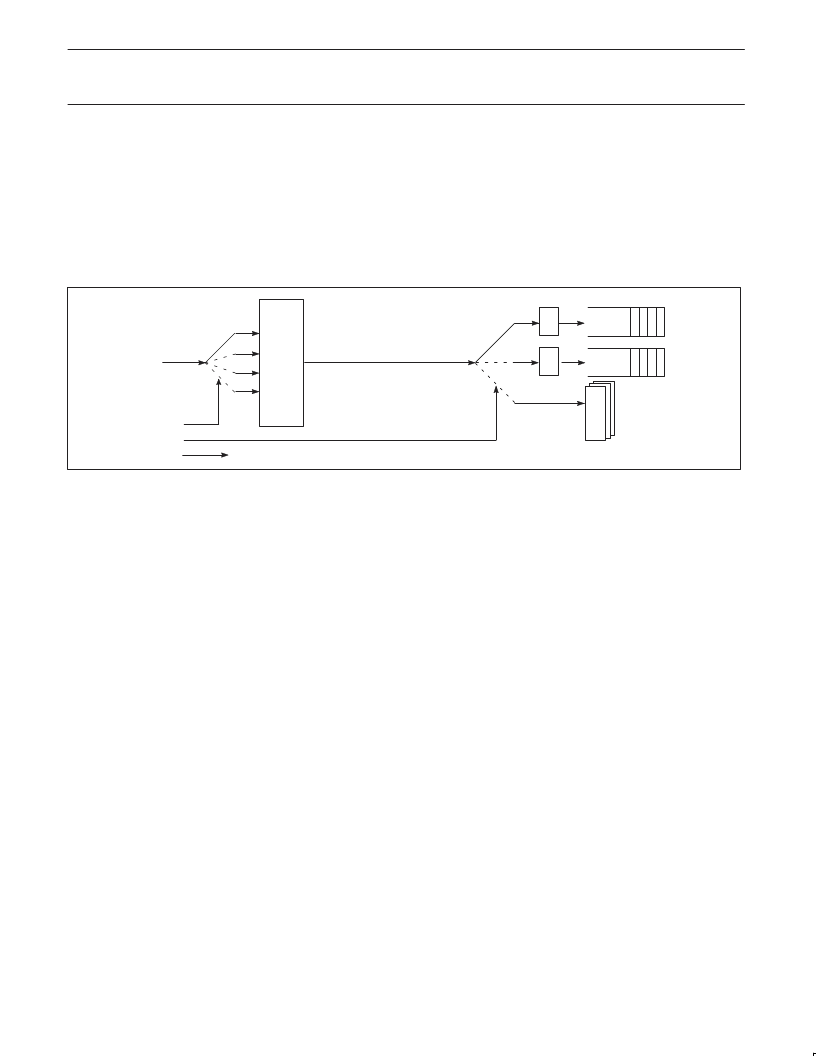
12.5.2
To write to an internal register the host interface must collect the 4 byte values (8 bit mode) or 2 word values (16 bit mode) into a 32 bit value
and then write the result to the target register in a single clock tick. This requires a register to hold the 32 bit value being compiled until it is
ready to be written to the actual target register. This temporary register inside the host interface is called the
shadow register
. In 8 bit mode,
address lines HIF A0 and HIF A1 are used to select which of the 4 bytes of the shadow register is to be written with the value on the CPU data
bus. In 16 bit mode, HIF A1 is used to select which half of the shadow register is to be written with the value on the CPU data bus. Only one
byte (8 bit mode) or one word (16 bit mode) can be written in a single write access cycle.
Write accesses
Not all registers can be accessed in Direct Address Space. Some of the registers are in an indirect address space, these registers control the
FIFO size and content protection system. The correct internal register space has to be selected through the host interface, using directly
addressable registers INDADDR (0x0F8) and INDDATA (0x0FC).
UPDATE/COPY CONTROL
HIF A8
HIF A2..7
HIF A0..1 (8 BIT MODE)
HIF A1 (16 BIT MODE)
CPU
S
8/16
32
32
REGISTERS
TR
Q
Q
MUX
MUX
SV01035
NOTES:
1. It is not required to write all 4 bytes, or both words of a register: those bytes that are either reserved (undefined) or don’t care do not have
to be written in which case they will be assigned the value that was left in the corresponding byte of the
shadow register
from a previous
write access. For example, to acknowledge an interrupt for the isochronous receiver in 8 bit mode, a single byte write to location
0x100+(0x4C)+3 = 0x14F is sufficient. The value 256 represents setting HIF A8=1. The host interface cannot directly access the FIFOs, but
instead reads from/writes into a transfer register (shown as TR in the Figures above). Data is moved between FIFO and TR by internal logic
as soon as possible without CPU intervention.
2. The update control line does not necessarily have to be connected to the CPU address line HIF A8. This input could also be controlled by
other means, for example a combinatorial circuit that activates the update control line whenever a write access is done for byte 3 or the
upper 16 bits. This makes the internal updating automatic for quadlet writing.
3. Writing the bytes or words of the shadow register can be done in any order and as often as needed (new writes simply overwrite the old
value).
4. It is now possible to read/modify/write a register using the shadow register (0x0F4) without rewriting all 4 bytes. For example, to modify an
enable bit in the fourth byte of the Asynchronous Interrupt Enable (0x0A4), a read of location 0x100+0x0A0+3=0x1A3, followed by a write of
the modified byte to the same location 0x100+0x0A0+3=0x1A3 is sufficient. The other bytes remain unchanged.
相關(guān)PDF資料 |
PDF描述 |
|---|---|
| PDI1394P21 | 3-port Physical Layer Interface(三端口物理層接口) |
| PDI1394P22 | 3-port Physical Layer Interface(三端口物理層接口) |
| PDI1394P24 | 2-port 400 Mbps physical layer interface(2端口 400 Mbps物理層接口) |
| PDI40C1D00 | |
| PDI40C1300 | |
相關(guān)代理商/技術(shù)參數(shù) |
參數(shù)描述 |
|---|---|
| PDI1394L41BE | 制造商:PHILIPS 制造商全稱:NXP Semiconductors 功能描述:1394 content protection AV link layer controller |
| PDI1394P11 | 制造商:PHILIPS 制造商全稱:NXP Semiconductors 功能描述:3-port physical layer interface |
| PDI1394P11A | 制造商:PHILIPS 制造商全稱:NXP Semiconductors 功能描述:3-port physical layer interface |
| PDI1394P11ABD | 制造商:PHILIPS 制造商全稱:NXP Semiconductors 功能描述:3-port physical layer interface |
| PDI1394P11ABD-S | 制造商:未知廠家 制造商全稱:未知廠家 功能描述:Transceiver |
發(fā)布緊急采購,3分鐘左右您將得到回復。