- 您現(xiàn)在的位置:買(mǎi)賣(mài)IC網(wǎng) > PDF目錄373631 > TFRA08C13 Ultraframer DS3/E3/DS2/E2/DS1/E1/DS0 PDF資料下載
參數(shù)資料
| 型號(hào): | TFRA08C13 |
| 元件分類(lèi): | 通信及網(wǎng)絡(luò) |
| 英文描述: | Ultraframer DS3/E3/DS2/E2/DS1/E1/DS0 |
| 中文描述: | Ultraframer DS3/E3/DS2/E2/DS1/E1/DS0 |
| 文件頁(yè)數(shù): | 109/188頁(yè) |
| 文件大?。?/td> | 3047K |
| 代理商: | TFRA08C13 |
第1頁(yè)第2頁(yè)第3頁(yè)第4頁(yè)第5頁(yè)第6頁(yè)第7頁(yè)第8頁(yè)第9頁(yè)第10頁(yè)第11頁(yè)第12頁(yè)第13頁(yè)第14頁(yè)第15頁(yè)第16頁(yè)第17頁(yè)第18頁(yè)第19頁(yè)第20頁(yè)第21頁(yè)第22頁(yè)第23頁(yè)第24頁(yè)第25頁(yè)第26頁(yè)第27頁(yè)第28頁(yè)第29頁(yè)第30頁(yè)第31頁(yè)第32頁(yè)第33頁(yè)第34頁(yè)第35頁(yè)第36頁(yè)第37頁(yè)第38頁(yè)第39頁(yè)第40頁(yè)第41頁(yè)第42頁(yè)第43頁(yè)第44頁(yè)第45頁(yè)第46頁(yè)第47頁(yè)第48頁(yè)第49頁(yè)第50頁(yè)第51頁(yè)第52頁(yè)第53頁(yè)第54頁(yè)第55頁(yè)第56頁(yè)第57頁(yè)第58頁(yè)第59頁(yè)第60頁(yè)第61頁(yè)第62頁(yè)第63頁(yè)第64頁(yè)第65頁(yè)第66頁(yè)第67頁(yè)第68頁(yè)第69頁(yè)第70頁(yè)第71頁(yè)第72頁(yè)第73頁(yè)第74頁(yè)第75頁(yè)第76頁(yè)第77頁(yè)第78頁(yè)第79頁(yè)第80頁(yè)第81頁(yè)第82頁(yè)第83頁(yè)第84頁(yè)第85頁(yè)第86頁(yè)第87頁(yè)第88頁(yè)第89頁(yè)第90頁(yè)第91頁(yè)第92頁(yè)第93頁(yè)第94頁(yè)第95頁(yè)第96頁(yè)第97頁(yè)第98頁(yè)第99頁(yè)第100頁(yè)第101頁(yè)第102頁(yè)第103頁(yè)第104頁(yè)第105頁(yè)第106頁(yè)第107頁(yè)第108頁(yè)當(dāng)前第109頁(yè)第110頁(yè)第111頁(yè)第112頁(yè)第113頁(yè)第114頁(yè)第115頁(yè)第116頁(yè)第117頁(yè)第118頁(yè)第119頁(yè)第120頁(yè)第121頁(yè)第122頁(yè)第123頁(yè)第124頁(yè)第125頁(yè)第126頁(yè)第127頁(yè)第128頁(yè)第129頁(yè)第130頁(yè)第131頁(yè)第132頁(yè)第133頁(yè)第134頁(yè)第135頁(yè)第136頁(yè)第137頁(yè)第138頁(yè)第139頁(yè)第140頁(yè)第141頁(yè)第142頁(yè)第143頁(yè)第144頁(yè)第145頁(yè)第146頁(yè)第147頁(yè)第148頁(yè)第149頁(yè)第150頁(yè)第151頁(yè)第152頁(yè)第153頁(yè)第154頁(yè)第155頁(yè)第156頁(yè)第157頁(yè)第158頁(yè)第159頁(yè)第160頁(yè)第161頁(yè)第162頁(yè)第163頁(yè)第164頁(yè)第165頁(yè)第166頁(yè)第167頁(yè)第168頁(yè)第169頁(yè)第170頁(yè)第171頁(yè)第172頁(yè)第173頁(yè)第174頁(yè)第175頁(yè)第176頁(yè)第177頁(yè)第178頁(yè)第179頁(yè)第180頁(yè)第181頁(yè)第182頁(yè)第183頁(yè)第184頁(yè)第185頁(yè)第186頁(yè)第187頁(yè)第188頁(yè)
Lucent Technologies Inc.
109
Preliminary Data Sheet
October 2000
TFRA08C13 OCTAL T1/E1 Framer
JTAG Boundary-Scan Specification
(continued)
Instruction Register
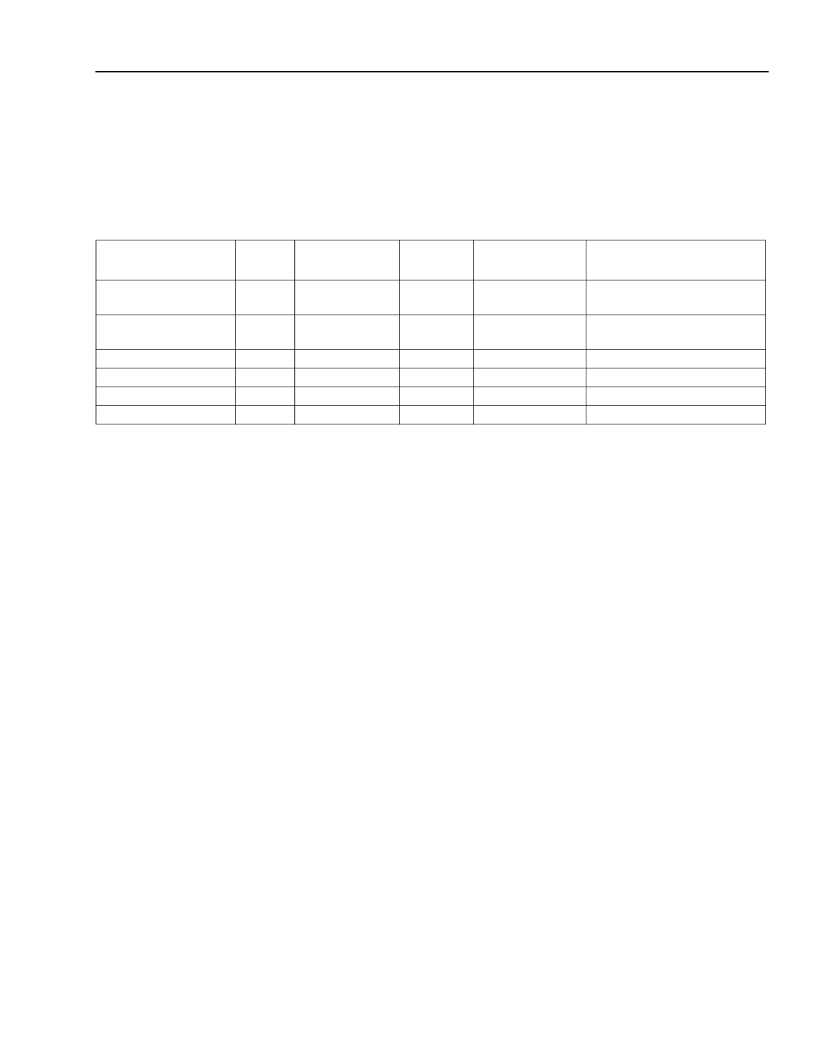
The instruction register (IR) is 4 bits in length. Table 49 shows the BS instructions implemented by the
TFRA08C13.
Table 49. TFRA08C13’s Boundary-Scan Instructions
Instruction
Code
Act. Register
TDI
→
TDO
Boundary Scan
Mode
Function
Output Defined Via
EXTEST
0000
TEST
Test external
connections
Read Manuf.
Register
3-state
Sample/load
Min. shift path
—
BS Register
IDCODE
0001
Identification
NORMAL
Core Logic
HIGHZ
0100
0101
1111
—
BYPASS
Boundary Scan
BYPASS
BYPASS
X
Output—High Impedance
Core Logic
Core Logic
Output—High Impedance
SAMPLE/PRELOAD
BYPASS
EVERYTHING ELSE
NORMAL
NORMAL
X
The instructions not supported in TFRA08C13 are
INTEST, RUNBIST, TOGGLE. A fixed binary 0001 pat-
tern (the 1 into the least significant bit) is loaded into
the IR in the capture-IR controller state. The IDCODE
instruction (binary 0001) is loaded into the IR during
the test-logic-reset controller state and at powerup.
The following is an explanation of the instructions sup-
ported by TFRA08C13 and their effect on the devices'
pins.
EXTEST
This instruction enables the path cells, the pins of the
ICs, and the connections between ASICs to be tested
via the circuit board. The test data can be loaded in the
chosen position of the BS register by means of the
SAMPLE/PRELOAD instruction. The EXTEST instruc-
tion selects the BS register as the test data register.
The data at the function inputs is clocked into the BS
register on the rising edge of TCK in the CAPTURE-DR
state. The contents of the BS register can be clocked
out via TDO in the SHIFT-DR state. The value of the
function outputs is solely determined by the contents of
the data clocked into the BS register and only changes
in the UPDATE-DR state on the falling edge of TCK.
DCODE
Information regarding the manufacturer’s ID for Lucent,
the IC number, and the version number can be read out
serially by means of the IDCODE instruction. The
IDCODE register is selected, and the BS register is set
to normal mode in the UPDATE-IR state. The IDCODE
is loaded at the rising edge of TCK in the CAPTURE-
DR state. The IDCODE register is read out via TDO in
the SHIFT-DR state.
HIGHZ
All 3-statable outputs are forced to a high-impedance
state, and all bidirectional ports to an input state by
means of the HIGHZ instruction. The impedance of the
outputs is set to high in the UPDATE-IR state. The func-
tion outputs are only determined in accordance with
another instruction if a different instruction becomes
active in the UPDATE-IR state. The BYPASS register is
selected as the test data register. The HIGHZ instruc-
tion is implemented in a similar manner to that used for
the BYPASS instruction.
SAMPLE/PRELOAD
The SAMPLE/PRELOAD instruction enables all the
input and output pins to be sampled during operation
(SAMPLE) and the result to be output via the shift
chain. This instruction does not impair the internal logic
functions. Defined values can be serially loaded in the
BS cells via TDI while the data is being output (PRE-
LOAD).
相關(guān)PDF資料 |
PDF描述 |
|---|---|
| TFRA08C13 | Ultraframer DS3/E3/DS2/E2/DS1/E1/DS0 |
| TFS380C | VI TELEFILTER Filter specification |
| TFT0675F | Anti-Aliasing and Reconstruction TFT range |
| TFT0675S | Anti-Aliasing and Reconstruction TFT range |
| TFT1350F | Anti-Aliasing and Reconstruction TFT range |
相關(guān)代理商/技術(shù)參數(shù) |
參數(shù)描述 |
|---|---|
| TFRA08C13-DB | 制造商:AGERE 制造商全稱(chēng):AGERE 功能描述:TFRA08C13 OCTAL T1/E1 Framer |
| TFRA28J133BAL-1 | 制造商:未知廠家 制造商全稱(chēng):未知廠家 功能描述:Telecomm/Datacomm |
| TFRA84J13 | 制造商:AGERE 制造商全稱(chēng):AGERE 功能描述:Ultraframer DS3/E3/DS2/E2/DS1/E1/DS0 |
| TFRA84J131BL-3-DB | 制造商:LSI Corporation 功能描述:Framer DS0/DS1/DS2/DS3/E1/E2/E3 1.5V/3.3V 909-Pin BGA |
| TFRA84J13DS0 | 制造商:AGERE 制造商全稱(chēng):AGERE 功能描述:Ultraframer DS3/E3/DS2/E2/DS1/E1/DS0 |
發(fā)布緊急采購(gòu),3分鐘左右您將得到回復(fù)。