- 您現(xiàn)在的位置:買賣IC網(wǎng) > PDF目錄361836 > WEDPNF8M721V-XBX 8Mx72 Synchronous DRAM + 8Mb Flash Mixed Module(8Mx72同步動(dòng)態(tài)RAM+8M位閃速存儲(chǔ)器混合型模塊) PDF資料下載
參數(shù)資料
| 型號(hào): | WEDPNF8M721V-XBX |
| 英文描述: | 8Mx72 Synchronous DRAM + 8Mb Flash Mixed Module(8Mx72同步動(dòng)態(tài)RAM+8M位閃速存儲(chǔ)器混合型模塊) |
| 中文描述: | 8Mx72同步DRAM 8MB閃存的混合模塊(8Mx72同步動(dòng)態(tài)RAM的800萬(wàn)位閃速存儲(chǔ)器混合型模塊) |
| 文件頁(yè)數(shù): | 27/42頁(yè) |
| 文件大小: | 686K |
| 代理商: | WEDPNF8M721V-XBX |
第1頁(yè)第2頁(yè)第3頁(yè)第4頁(yè)第5頁(yè)第6頁(yè)第7頁(yè)第8頁(yè)第9頁(yè)第10頁(yè)第11頁(yè)第12頁(yè)第13頁(yè)第14頁(yè)第15頁(yè)第16頁(yè)第17頁(yè)第18頁(yè)第19頁(yè)第20頁(yè)第21頁(yè)第22頁(yè)第23頁(yè)第24頁(yè)第25頁(yè)第26頁(yè)當(dāng)前第27頁(yè)第28頁(yè)第29頁(yè)第30頁(yè)第31頁(yè)第32頁(yè)第33頁(yè)第34頁(yè)第35頁(yè)第36頁(yè)第37頁(yè)第38頁(yè)第39頁(yè)第40頁(yè)第41頁(yè)第42頁(yè)
27
White Electronic Designs Corporation (602) 437-1520 www.whiteedc.com
WEDPNF8M721V-XBX
FD
5
: Exceeded Timing Limits
FD
5
will indicate whether the program or erase time has exceeded
the specified limits (internal pulse count). Under these conditions
FD
5
will produce a “1”. This is a failure condition that indicates the
program or erase cycle was not successfully completed.
The FD
5
failure condition may appear if the system tries to
program a “1” to a location that is previously programmed to “0.”
Only an erase operation can change a “0” back to a “1.” Under this
condition, the device halts the operation, and when the operation
has exceeded timing limits, the FD
5
bit will produce a “1”.
Under both these conditions, the system must issue the reset
command to return the device to reading array data.
FD
3
: Sector Erase Timer
After writing a sector erase command sequence, the system may
read FD
3
to determine whether or not an erase operation has
begun. (The sector erase timer does not apply to the chip erase
command.) If additional sectors are selected for erasure, the
entire time-out also applies after each additional sector erase
command. When the time-out is completed, FD
3
switches from
“0” to “1.” The system may ignore FD
3
if the system can guarantee
that the time between additional sector erase commands will
always be less than 50
μ
s. See also the “Sector Command Se-
quence” section.
After the sector erase command sequence is written, the system
should read the status on FD
7
(Data Polling) or FD
6
(Toggle Bit I) to
ensure the device has accepted the command sequence, and then
read FD
3
. If FD
3
is high (“1”) the internally controlled erase cycle
has begun; all further commands (other than Erase Suspend) will
be ignored until the erase operation is completed. If FD
3
is low
(“0”), the device will accept additional sector erase commands. To
ensure the command has been accepted, the system software
should check the status of FD
3
prior to and following each subse-
quent sector erase command. If FD
3
is high on the second status
check, the last command may not have been accepted. Table 8
shows the outputs for FD
3
.
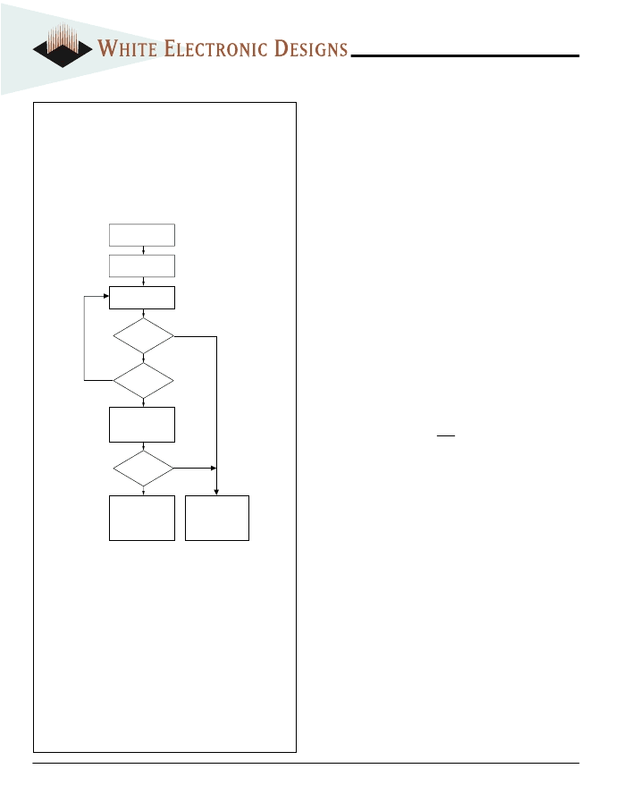
FIG. 9
TOGGLE BIT ALGORITHM
1. Read toggle bit twice to detemine whether or not it is toggling. See text.
2. Recheck toggle bit because it may stop toggling as FD
5
changes to 1. See
text.
Start
Read Byte
(FD0-FD7)
Read Byte
(FD0-FD7) (1)
Read Byte
(FD0-FD7) (1,2)
Twice
Program/Erase
Operaton Not
Complete, Write
Reset Command
Toggle Bit
= Toggle
FD5 = 1
Toggle Bit
= Toggle
No
Yes
Yes
Yes
No
Program/Erase
Operaton
Complete
No
相關(guān)PDF資料 |
PDF描述 |
|---|---|
| WEDPNF8M722V-XBX | 8Mx72 Synchronous DRAM + 16Mb Flash Mixed Module(8Mx72同步動(dòng)態(tài)RAM+16M位閃速存儲(chǔ)器混合型模塊) |
| WEDPS512K32V-XBX | SRAM MCP |
| WEDPS512K32-XBX | SRAM MCP |
| WEDPY256K72V-XBX | SSRAM MCP |
| WEDPZ512K72S-XBX | NBL SSRAM MCP |
相關(guān)代理商/技術(shù)參數(shù) |
參數(shù)描述 |
|---|---|
| WEDPNF8M722V-1010BC | 制造商:WEDC 制造商全稱:White Electronic Designs Corporation 功能描述:8Mx72 Synchronous DRAM + 16Mb Flash Mixed Module Multi-Chip Package |
| WEDPNF8M722V-1010BI | 制造商:WEDC 制造商全稱:White Electronic Designs Corporation 功能描述:8Mx72 Synchronous DRAM + 16Mb Flash Mixed Module Multi-Chip Package |
| WEDPNF8M722V-1010BM | 制造商:WEDC 制造商全稱:White Electronic Designs Corporation 功能描述:8Mx72 Synchronous DRAM + 16Mb Flash Mixed Module Multi-Chip Package |
| WEDPNF8M722V-1012BC | 制造商:WEDC 制造商全稱:White Electronic Designs Corporation 功能描述:8Mx72 Synchronous DRAM + 16Mb Flash Mixed Module Multi-Chip Package |
| WEDPNF8M722V-1012BI | 制造商:WEDC 制造商全稱:White Electronic Designs Corporation 功能描述:8Mx72 Synchronous DRAM + 16Mb Flash Mixed Module Multi-Chip Package |
發(fā)布緊急采購(gòu),3分鐘左右您將得到回復(fù)。