- 您現(xiàn)在的位置:買(mǎi)賣(mài)IC網(wǎng) > PDF目錄366329 > ACE9050 (Mitel Networks Corporation) System Controller and Data Modem(為蜂窩式手機(jī)提供控制和邏輯接口功能的系統(tǒng)控制器和數(shù)據(jù)調(diào)制解調(diào)器) PDF資料下載
參數(shù)資料
| 型號(hào): | ACE9050 |
| 廠商: | Mitel Networks Corporation |
| 英文描述: | System Controller and Data Modem(為蜂窩式手機(jī)提供控制和邏輯接口功能的系統(tǒng)控制器和數(shù)據(jù)調(diào)制解調(diào)器) |
| 中文描述: | 系統(tǒng)控制器和數(shù)據(jù)調(diào)制解調(diào)器(為蜂窩式手機(jī)提供控制和邏輯接口功能的系統(tǒng)控制器和數(shù)據(jù)調(diào)制解調(diào)器) |
| 文件頁(yè)數(shù): | 19/52頁(yè) |
| 文件大?。?/td> | 366K |
| 代理商: | ACE9050 |
第1頁(yè)第2頁(yè)第3頁(yè)第4頁(yè)第5頁(yè)第6頁(yè)第7頁(yè)第8頁(yè)第9頁(yè)第10頁(yè)第11頁(yè)第12頁(yè)第13頁(yè)第14頁(yè)第15頁(yè)第16頁(yè)第17頁(yè)第18頁(yè)當(dāng)前第19頁(yè)第20頁(yè)第21頁(yè)第22頁(yè)第23頁(yè)第24頁(yè)第25頁(yè)第26頁(yè)第27頁(yè)第28頁(yè)第29頁(yè)第30頁(yè)第31頁(yè)第32頁(yè)第33頁(yè)第34頁(yè)第35頁(yè)第36頁(yè)第37頁(yè)第38頁(yè)第39頁(yè)第40頁(yè)第41頁(yè)第42頁(yè)第43頁(yè)第44頁(yè)第45頁(yè)第46頁(yè)第47頁(yè)第48頁(yè)第49頁(yè)第50頁(yè)第51頁(yè)第52頁(yè)

ACE9050
19
AS
Address Strobe (pin 5)
This input is used in Emulation Mode only. Th external D [7:0] will
contain both data and the lower 8 bits of the address bus.The Bus
Interface provides the transparent latch required to hold the
value of the address during the latter part of the cycle. The AS is
provided to control the Latch Enable. In a typical system this will
be directly connected to the emulating 6303 AS output.
R/W
Read/Not Write (pin 95)
This is an output in Normal mode, but an input in Emulation
Mode. It is the processor Read/Not Write line. The timing of this
output is not guaranteed to be the same as a standard 6303
processor. In Emulation mode it will be directly connected to the
Emulating 6303 R/W line.
D [7:0]
Data (and Address in Emulation mode) (Pins 18-25)
In Normal mode these pins provide bidirectional data transfer
between the ACE9050 6303 and external memory. In Emulation
mode they provide the directional data and the lower 8 bits of the
address bus into the ACE9050.
A [7:0]
Lower 8 address bits (Pins 40, 39, 35-30)
These outputs provide the lower 8 bits of the address bus for
external memory. This is the case for both Normal and Emulation
modes.
A [13:8]
Address Bits 13 to 8 (pins 46-41)
In Normal mode these provide the output of the ACE9050
6303 address bus bits 13 to 8, for addressing external devices.
In Emulation mode, A[13:8] provide input for an external 6303
address bus, to address the ACE9050 functions excluding the
6303.
A [15:14]
Emulation Address bits 15 and 14 (pins 92 and 93)
These inputs are only used in Emulation mode. The
internal 6303 address A[15:14] are fed to the banked address
logic and not to an external pin. In emulation mode the host
processor must drive the complete 6303 internal address bus
so A[15:14] inputs are provided. The host processor will then
drive the entire internal bus and the bank select register, so
the external memory access will be the same regardless of
Emulation or Normal mode.
BA [17:14]
Banked address (pins 50 to 47)
The ACE9050 expands the external address bus to 18 bits.
This allows up to 256K of memory space. BA [17:14] are the
outputs from the bank select register. The operation of the
refister is described further in ‘Memory Map and Banked
Addressing’, below.
CSEPN
Chip Select (pin 28)
This output provides active low chip select for accessing
external program memory. On reset the entire external memory
address space is mapped to CSEPN. In the Banked area of the
memory map the programmer can select either CSEPN or
CSE2N access via bit 4 of the Bank Select register.
CSE2N
Chip Select (pin 29)
This output provides an active low chip select for accessing
external memory or other suitable device. In the Banked area of
the memory map the programmer can select either CSEPN or
CSE2N access via bit 4 of the Bank Select register.
V
DDM
Supply to Memory Interface (pin 38)
The power supply pin for the memory interface, V
DDM
,
provides the power supply for the following pads:
A [13:0], BA [17:14], D [7:0], CSEPN, CSE2N, WEN and OEN
Memory Map and Banked Addressing
The ACE9050 provides the circuitry to create a banked
addressing system which will ncrease the size of the programming
space from 16 bit (64K bytes) to 18 bit (256K Bytes) and enable
two Chip Select lines to be programmed. This is achieved using
an internal register to select the required page of memory and
chip select line.
The use of banked addressing and associated circuitry is not
mandatory in a system using an ACE9050.
When using banked addressing the external addresses
generated and thus the system memory map are different from
the 6303 memory map. The banked addressing functions in the
same manner for both Normal and Emulation mode with a
external processor.
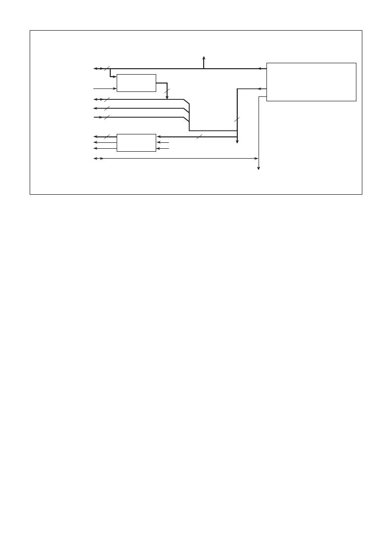
Fig. 13 Data and Address bus configuration
ACE9050 6303
AND KERNEL
ID[7:0]
(DISABLED IN EMULATION MODE)
AD[15:0]
IRW
(DISABLED IN EMULATION MODE)
TRANSPARENT
LATCH
LATCH ENABLE
MEMORY
BANK
SWITCHING
INTERNAL
ADDRESS BUS [15:0]
NOEMUL:
NOEMUL:
[7:0]
[13:8]
[15:14]
DATA BUS
INTERNAL EPROM
[15:14]
A[13:8] OUTPUT
NOT USED
A7:0
BA[17:14]
CSEPN
CSE2N
NOEMUL:
R/W NOT USED
R/W INPUT
4
2
6
8
8
NOEMUL:
NOT USED
NOEMUL:
D[7:0]
16
2
INTERNAL
READ /NOT WRITE
8
INTERNAL
DATA BUS [7:0]
相關(guān)PDF資料 |
PDF描述 |
|---|---|
| ACE9050 | System Controller and Data Modem Advance Information |
| ACFA-450 | AM CERAMIC FILTERS |
| ACFA-455 | AM CERAMIC FILTERS |
| ACFA-459 | AM CERAMIC FILTERS |
| ACFA-468 | AM CERAMIC FILTERS |
相關(guān)代理商/技術(shù)參數(shù) |
參數(shù)描述 |
|---|---|
| ACE9050C/IW/FP1N | 制造商:Microsemi Corporation 功能描述:PB FREE SYSTEM CONTROLLER & DATA MODEM - Bulk |
| ACE9050C/IW/FP1Q | 制造商:Microsemi Corporation 功能描述:PB FREE SYSTEM CONTROLLER & DATA MODEM - Bulk |
| ace9050c/iw/fp8q | 制造商:Rochester Electronics LLC 功能描述: 制造商:Zarlink Semiconductor Inc 功能描述: |
| ace9050d/ig/gp1n | 制造商:Microsemi Corporation 功能描述:CNTRLR AND DATA MODEM 100LQFP - Bulk 制造商:Rochester Electronics LLC 功能描述: 制造商:Zarlink Semiconductor Inc 功能描述: |
| ACE9050D/IG/GP2N | 制造商:Microsemi Corporation 功能描述:CNTRLR AND DATA MODEM 100LQFP - Bulk |
發(fā)布緊急采購(gòu),3分鐘左右您將得到回復(fù)。