- 您現(xiàn)在的位置:買賣IC網(wǎng) > PDF目錄296408 > M58WR064EB85ZB6T (NUMONYX) 4M X 16 FLASH 1.8V PROM, 85 ns, PBGA56 PDF資料下載
參數(shù)資料
| 型號: | M58WR064EB85ZB6T |
| 廠商: | NUMONYX |
| 元件分類: | PROM |
| 英文描述: | 4M X 16 FLASH 1.8V PROM, 85 ns, PBGA56 |
| 封裝: | 7.70 X 9 MM, 0.75 MM PITCH, VFBGA-56 |
| 文件頁數(shù): | 58/81頁 |
| 文件大?。?/td> | 539K |
| 代理商: | M58WR064EB85ZB6T |
第1頁第2頁第3頁第4頁第5頁第6頁第7頁第8頁第9頁第10頁第11頁第12頁第13頁第14頁第15頁第16頁第17頁第18頁第19頁第20頁第21頁第22頁第23頁第24頁第25頁第26頁第27頁第28頁第29頁第30頁第31頁第32頁第33頁第34頁第35頁第36頁第37頁第38頁第39頁第40頁第41頁第42頁第43頁第44頁第45頁第46頁第47頁第48頁第49頁第50頁第51頁第52頁第53頁第54頁第55頁第56頁第57頁當(dāng)前第58頁第59頁第60頁第61頁第62頁第63頁第64頁第65頁第66頁第67頁第68頁第69頁第70頁第71頁第72頁第73頁第74頁第75頁第76頁第77頁第78頁第79頁第80頁第81頁
61/81
M58WR064ET, M58WR064EB
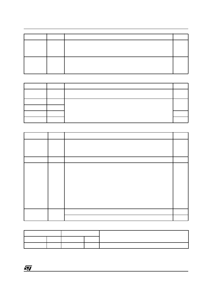
Table 35. Protection Register Information
Table 36. Burst Read Information
Table 37. Bank and Erase Block Region Information
Note: 1. The variable P is a pointer which is defined at CFI offset 15h.
2. Bank Regions. There are two Bank Regions, 1 contains all the banks that are made up of main blocks only, 2 contains the banks
that are made up of the parameter and main blocks.
(P+C)h = 45h
0018h
VDD Logic Supply Optimum Program/Erase voltage (highest performance)
bit 7 to 4HEX value in volts
bit 3 to 0BCD value in 100 mV
1.8V
(P+D)h = 46h
00C0h
VPP Supply Optimum Program/Erase voltage
bit 7 to 4HEX value in volts
bit 3 to 0BCD value in 100 mV
12V
Offset
Data
Description
Value
(P+E)h = 47h
0001h
Number of protection register fields in JEDEC ID space. 0000h indicates that
256 fields are available.
1
(P+F)h = 48h
0080h
Protection Field 1: Protection Description
Bits 0-7 Lower byte of protection register address
Bits 8-15 Upper byte of protection register address
Bits 16-23 2n bytes in factory pre-programmed region
Bits 24-31 2n bytes in user programmable region
0080h
(P+10)h = 49h
0000h
(P+11)h = 4Ah
0003h
8 Bytes
(P+12)h= 4Bh
0004h
16 Bytes
Offset
Data
Description
Value
(P+13)h = 4Ch
0003h
Page-mode read capability
bits 0-7
’n’ such that 2n HEX value represents the number of read-
page bytes. See offset 28h for device word width to
determine page-mode data output width.
8 Bytes
(P+14)h = 4Dh
0003h
Number of synchronous mode read configuration fields that follow.
3
(P+15)h = 4Eh
0001h
Synchronous mode read capability configuration 1
bit 3-7
Reserved
bit 0-2
’n’ such that 2n+1 HEX value represents the maximum
number of continuous synchronous reads when the device is
configured for its maximum word width. A value of 07h
indicates that the device is capable of continuous linear
bursts that will output data until the internal burst counter
reaches the end of the device’s burstable address space.
This field’s 3-bit value can be written directly to the read
configuration register bit 0-2 if the device is configured for its
maximum word width. See offset 28h for word width to
determine the burst data output width.
4
(P+16)h = 4Fh
0002h
Synchronous mode read capability configuration 2
8
(P+17)h = 50h
0007h
Synchronous mode read capability configuration 3
Cont.
M58WR064ET (top)
M58WR064EB (bottom)
Description
Offset
Data
Offset
Data
(P+18)h =51h
02h
(P+18)h =51h
02h
Number of Bank Regions within the device
Offset
Data
Description
Value
相關(guān)PDF資料 |
PDF描述 |
|---|---|
| M58WR064KU70ZA6U | 4M X 16 FLASH 1.8V PROM, 70 ns, PBGA44 |
| M5L28FGNFREQ | CRYSTAL OSCILLATOR, CLOCK, 1.544 MHz - 125 MHz, HCMOS OUTPUT |
| M3L13TCNFREQ | CRYSTAL OSCILLATOR, CLOCK, 1.544 MHz - 125 MHz, HCMOS OUTPUT |
| M3L14FCNFREQ | CRYSTAL OSCILLATOR, CLOCK, 1.544 MHz - 125 MHz, HCMOS OUTPUT |
| M3L15TGNFREQ | CRYSTAL OSCILLATOR, CLOCK, 1.544 MHz - 125 MHz, HCMOS OUTPUT |
相關(guān)代理商/技術(shù)參數(shù) |
參數(shù)描述 |
|---|---|
| M58WR064EBZB | 制造商:STMICROELECTRONICS 制造商全稱:STMicroelectronics 功能描述:64 Mbit 4Mb x 16, Multiple Bank, Burst 1.8V Supply Flash Memory |
| M58WR064ET | 制造商:STMICROELECTRONICS 制造商全稱:STMicroelectronics 功能描述:64 Mbit 4Mb x 16, Multiple Bank, Burst 1.8V Supply Flash Memory |
| M58WR064ET10ZB6T | 制造商:STMICROELECTRONICS 制造商全稱:STMicroelectronics 功能描述:64 Mbit 4Mb x 16, Multiple Bank, Burst 1.8V Supply Flash Memory |
| M58WR064ET70ZB6T | 功能描述:閃存 64M (4Mx16) 70ns RoHS:否 制造商:ON Semiconductor 數(shù)據(jù)總線寬度:1 bit 存儲類型:Flash 存儲容量:2 MB 結(jié)構(gòu):256 K x 8 定時類型: 接口類型:SPI 訪問時間: 電源電壓-最大:3.6 V 電源電壓-最小:2.3 V 最大工作電流:15 mA 工作溫度:- 40 C to + 85 C 安裝風(fēng)格:SMD/SMT 封裝 / 箱體: 封裝:Reel |
| M58WR064ET80ZB6T | 制造商:STMICROELECTRONICS 制造商全稱:STMicroelectronics 功能描述:64 Mbit 4Mb x 16, Multiple Bank, Burst 1.8V Supply Flash Memory |
發(fā)布緊急采購,3分鐘左右您將得到回復(fù)。