- 您現(xiàn)在的位置:買(mǎi)賣(mài)IC網(wǎng) > PDF目錄296408 > M58WR064EB85ZB6T (NUMONYX) 4M X 16 FLASH 1.8V PROM, 85 ns, PBGA56 PDF資料下載
參數(shù)資料
| 型號(hào): | M58WR064EB85ZB6T |
| 廠商: | NUMONYX |
| 元件分類(lèi): | PROM |
| 英文描述: | 4M X 16 FLASH 1.8V PROM, 85 ns, PBGA56 |
| 封裝: | 7.70 X 9 MM, 0.75 MM PITCH, VFBGA-56 |
| 文件頁(yè)數(shù): | 60/81頁(yè) |
| 文件大?。?/td> | 539K |
| 代理商: | M58WR064EB85ZB6T |
第1頁(yè)第2頁(yè)第3頁(yè)第4頁(yè)第5頁(yè)第6頁(yè)第7頁(yè)第8頁(yè)第9頁(yè)第10頁(yè)第11頁(yè)第12頁(yè)第13頁(yè)第14頁(yè)第15頁(yè)第16頁(yè)第17頁(yè)第18頁(yè)第19頁(yè)第20頁(yè)第21頁(yè)第22頁(yè)第23頁(yè)第24頁(yè)第25頁(yè)第26頁(yè)第27頁(yè)第28頁(yè)第29頁(yè)第30頁(yè)第31頁(yè)第32頁(yè)第33頁(yè)第34頁(yè)第35頁(yè)第36頁(yè)第37頁(yè)第38頁(yè)第39頁(yè)第40頁(yè)第41頁(yè)第42頁(yè)第43頁(yè)第44頁(yè)第45頁(yè)第46頁(yè)第47頁(yè)第48頁(yè)第49頁(yè)第50頁(yè)第51頁(yè)第52頁(yè)第53頁(yè)第54頁(yè)第55頁(yè)第56頁(yè)第57頁(yè)第58頁(yè)第59頁(yè)當(dāng)前第60頁(yè)第61頁(yè)第62頁(yè)第63頁(yè)第64頁(yè)第65頁(yè)第66頁(yè)第67頁(yè)第68頁(yè)第69頁(yè)第70頁(yè)第71頁(yè)第72頁(yè)第73頁(yè)第74頁(yè)第75頁(yè)第76頁(yè)第77頁(yè)第78頁(yè)第79頁(yè)第80頁(yè)第81頁(yè)
63/81
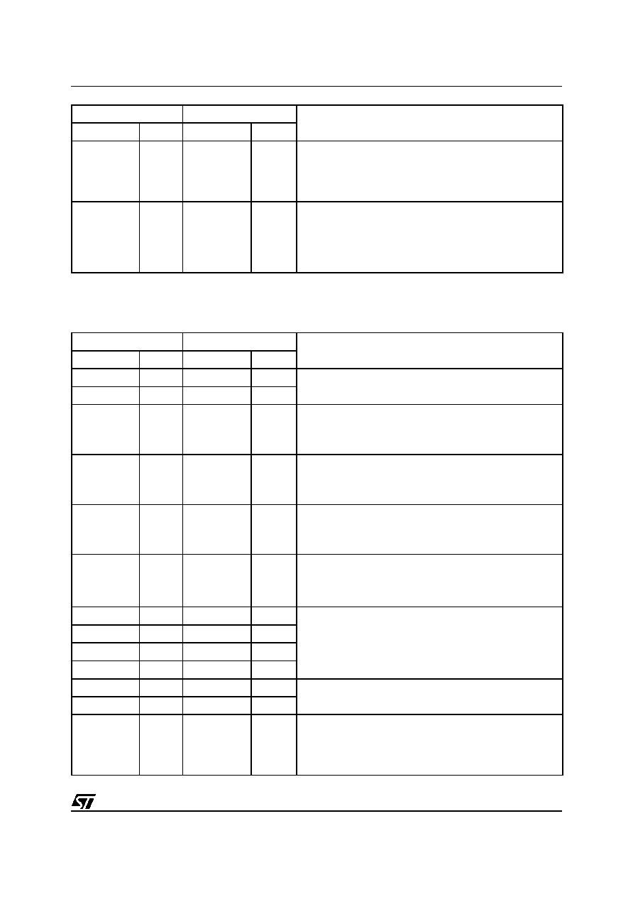
M58WR064ET, M58WR064EB
Note: 1. The variable P is a pointer which is defined at CFI offset 15h.
2. Bank Regions. There are two Bank Regions, 1 contains all the banks that are made up of main blocks only, 2 contains the banks
that are made up of the parameter and main blocks.
Table 39. Bank and Erase Block Region 2 Information
(P+2D)h =66h
01h
Bank Regions 1 (Erase Block Type 2): BIts per cell, internal
ECC
Bits 0-3: bits per cell in erase region
Bit 4: reserved for “internal ECC used”
BIts 5-7: reserved
(P+2E)h =67h
03h
Bank Region 1 (Erase Block Type 2): Page mode and
synchronous mode capabilities
Bit 0: Page-mode reads permitted
Bit 1: Synchronous reads permitted
Bit 2: Synchronous writes permitted
Bits 3-7: reserved
M58WR064ET (top)
M58WR064EB (bottom)
Description
Offset
Data
Offset
Data
(P+27)h =60h
01h
(P+2F)h =68h
0Fh
Number of identical banks within bank region 2
(P+28)h =61h
00h
(P+30)h =69h
00h
(P+29)h =62h
11h
(P+31)h =6Ah
11h
Number of program or erase operations allowed in bank region
2:
Bits 0-3: Number of simultaneous program operations
Bits 4-7: Number of simultaneous erase operations
(P+2A)h =63h
00h
(P+32)h =6Bh
00h
Number of program or erase operations allowed in other banks
while a bank in this region is programming
Bits 0-3: Number of simultaneous program operations
Bits 4-7: Number of simultaneous erase operations
(P+2B)h =64h
00h
(P+33)h =6Ch
00h
Number of program or erase operations allowed in other banks
while a bank in this region is erasing
Bits 0-3: Number of simultaneous program operations
Bits 4-7: Number of simultaneous erase operations
(P+2C)h =65h
02h
(P+34)h =6Dh
01h
Types of erase block regions in region 2
n = number of erase block regions with contiguous same-size
erase blocks.
Symmetrically blocked banks have one blocking region.(2)
(P+2D)h =66h
06h
(P+35)h =6Eh
07h
Bank Region 2 Erase Block Type 1 Information
Bits 0-15: n+1 = number of identical-sized erase blocks
Bits 16-31: n×256 = number of bytes in erase block region
(P+2E)h =67h
00h
(P+36)h =6Fh
00h
(P+2F)h =68h
00h
(P+37)h =70h
00h
(P+30)h =69h
01h
(P+38)h =71h
01h
(P+31)h =6Ah
64h
(P+39)h =72h
64h
Bank Region 2 (Erase Block Type 1)
Minimum block erase cycles × 1000
(P+32)h =6Bh
00h
(P+3A)h =73h
00h
(P+33)h =6Ch
01h
(P+3B)h =74h
01h
Bank Region 2 (Erase Block Type 1): BIts per cell, internal
ECC
Bits 0-3: bits per cell in erase region
Bit 4: reserved for “internal ECC used”
BIts 5-7: reserved
M58WR064ET (top)
M58WR064EB (bottom)
Description
Offset
Data
Offset
Data
相關(guān)PDF資料 |
PDF描述 |
|---|---|
| M58WR064KU70ZA6U | 4M X 16 FLASH 1.8V PROM, 70 ns, PBGA44 |
| M5L28FGNFREQ | CRYSTAL OSCILLATOR, CLOCK, 1.544 MHz - 125 MHz, HCMOS OUTPUT |
| M3L13TCNFREQ | CRYSTAL OSCILLATOR, CLOCK, 1.544 MHz - 125 MHz, HCMOS OUTPUT |
| M3L14FCNFREQ | CRYSTAL OSCILLATOR, CLOCK, 1.544 MHz - 125 MHz, HCMOS OUTPUT |
| M3L15TGNFREQ | CRYSTAL OSCILLATOR, CLOCK, 1.544 MHz - 125 MHz, HCMOS OUTPUT |
相關(guān)代理商/技術(shù)參數(shù) |
參數(shù)描述 |
|---|---|
| M58WR064EBZB | 制造商:STMICROELECTRONICS 制造商全稱(chēng):STMicroelectronics 功能描述:64 Mbit 4Mb x 16, Multiple Bank, Burst 1.8V Supply Flash Memory |
| M58WR064ET | 制造商:STMICROELECTRONICS 制造商全稱(chēng):STMicroelectronics 功能描述:64 Mbit 4Mb x 16, Multiple Bank, Burst 1.8V Supply Flash Memory |
| M58WR064ET10ZB6T | 制造商:STMICROELECTRONICS 制造商全稱(chēng):STMicroelectronics 功能描述:64 Mbit 4Mb x 16, Multiple Bank, Burst 1.8V Supply Flash Memory |
| M58WR064ET70ZB6T | 功能描述:閃存 64M (4Mx16) 70ns RoHS:否 制造商:ON Semiconductor 數(shù)據(jù)總線寬度:1 bit 存儲(chǔ)類(lèi)型:Flash 存儲(chǔ)容量:2 MB 結(jié)構(gòu):256 K x 8 定時(shí)類(lèi)型: 接口類(lèi)型:SPI 訪問(wèn)時(shí)間: 電源電壓-最大:3.6 V 電源電壓-最小:2.3 V 最大工作電流:15 mA 工作溫度:- 40 C to + 85 C 安裝風(fēng)格:SMD/SMT 封裝 / 箱體: 封裝:Reel |
| M58WR064ET80ZB6T | 制造商:STMICROELECTRONICS 制造商全稱(chēng):STMicroelectronics 功能描述:64 Mbit 4Mb x 16, Multiple Bank, Burst 1.8V Supply Flash Memory |
發(fā)布緊急采購(gòu),3分鐘左右您將得到回復(fù)。