- 您現(xiàn)在的位置:買賣IC網(wǎng) > PDF目錄383645 > MT90812 (Mitel Networks Corporation) Integrated Digital Switch (IDX)(集成數(shù)字開關(guān)) PDF資料下載
參數(shù)資料
| 型號: | MT90812 |
| 廠商: | Mitel Networks Corporation |
| 英文描述: | Integrated Digital Switch (IDX)(集成數(shù)字開關(guān)) |
| 中文描述: | 綜合數(shù)字交換機(IDX的)(集成數(shù)字開關(guān)) |
| 文件頁數(shù): | 16/105頁 |
| 文件大小: | 334K |
| 代理商: | MT90812 |
第1頁第2頁第3頁第4頁第5頁第6頁第7頁第8頁第9頁第10頁第11頁第12頁第13頁第14頁第15頁當前第16頁第17頁第18頁第19頁第20頁第21頁第22頁第23頁第24頁第25頁第26頁第27頁第28頁第29頁第30頁第31頁第32頁第33頁第34頁第35頁第36頁第37頁第38頁第39頁第40頁第41頁第42頁第43頁第44頁第45頁第46頁第47頁第48頁第49頁第50頁第51頁第52頁第53頁第54頁第55頁第56頁第57頁第58頁第59頁第60頁第61頁第62頁第63頁第64頁第65頁第66頁第67頁第68頁第69頁第70頁第71頁第72頁第73頁第74頁第75頁第76頁第77頁第78頁第79頁第80頁第81頁第82頁第83頁第84頁第85頁第86頁第87頁第88頁第89頁第90頁第91頁第92頁第93頁第94頁第95頁第96頁第97頁第98頁第99頁第100頁第101頁第102頁第103頁第104頁第105頁
MT90812
Advance Information
12
5.0
Address Memory Map
The MT90812 memory is accessed via the microport. The microport can operate in multiplexed or non-
multiplexed mode as described in “Microprocessor Port” on page 49 The access to the MT90812 memory for
multiplexed and non-multiplexed mode is described below.
5.1
Memory Page Select
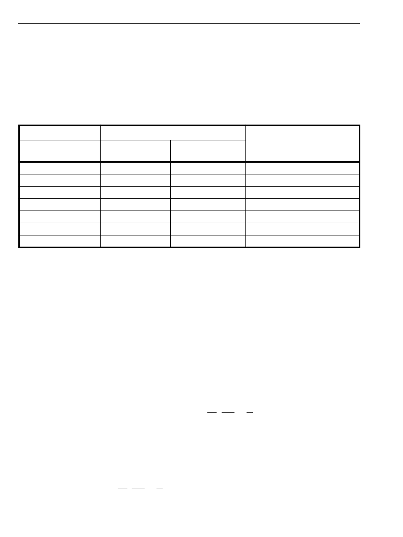
The MT90812 memory is divided into 7 pages, as listed in Table 1.
In multiplexed mode, the Memory Select bits in the Address Memory Select register (AMS) determine the page
that is addressed. In non-multiplexed mode, the external address bits A9,A8,A7, determine the page that is
addressed, eliminating the need to access the AMS register for memory page select.
The control registers, described in “Detailed Register Descriptions” on page 52, consist of one page of 128
locations. In multiplexed mode the control registers are accessed independent of the setting of the memory
select bits in the AMS register, by setting the external address bit A7 to low. In non-multiplexed model the
control registers are accessed by setting address bits A9, A8, and A7 to High.
The control register at
location 61
H
( 3E1
H
in motorola non-muxed, 061
H
in in multiplexed mode) must be initialized to 080
H
.
The addressing of the other blocks and memory pages are described below. Each Data and Connect Memory
page consists of 128 locations, as shown in Table 2.
5.1.1
An MT90812 memory address, in multiplexed microport mode, consists of two portions. The higher order
bits(3) originate from the Control Address Memory Select (AMS) register, which may be written to or read from
via the Control Interface. The Control Interface receives address information at A7 to A0, data information at
D7 to D0 and handles the microprocessor control signals CS, DTA, R/W and DS. The lower order bits(8)
originate from the address lines directly. The address lines A6-A0, on the Control Interface, give access to the
MT90812 registers directly if A7 is zero, or depending on the contents of AMS register, to the High or Low
sections of the Connection Memory, or to the Data Memory.
Addressing Memory Pages in Multiplexed Microport Mode
5.1.2
A MT90812 memory address, in
non-multiplexed
microport mode, consists of A9 to A0. The higher order
bits(3) originating from the external address bits A9,A8,A7, control which page is accessed. The Control
Interface receives address information at A9 to A0, data information at D7 to D0 and handles the
microprocessor control signals CS, DTA, R/W and DS. The lower order bits(7) originating from the external
Addressing Memory Pages in Non-Multiplexed Microport Mode.
Non-Multiplexed Mode
Multiplexed Mode
Memory Pages
External Address
A9,A8,A7
Memory Select Bits
External Address A7
111
XXX
0
Control Registers (Section 22.0)
000
000
1
Local Data Memory
001
001
1
Expansion Data Memory
010
010
1
Local Connect Memory Low
011
011
1
Expansion Connect Memory Low
100
100
1
Local Connect Memory High
101
101
1
Expansion Connect Memory High
Table 1 - MT90812 Memory Page Select
相關(guān)PDF資料 |
PDF描述 |
|---|---|
| MT90840AK | Distributed Hyperchannel Switch |
| MT90840AP | Distributed Hyperchannel Switch |
| MT9085B | PAC - Parallel Access Circuit(并行存取電路) |
| MT9092 | Digital Telephone with HDLC(數(shù)字電話(帶高階數(shù)據(jù)鏈路控制HDLC)) |
| MT9092 | ISO2-CMOS ST-BUS⑩ FAMILY Digital Telephone with HDLC (HPhone-II) |
相關(guān)代理商/技術(shù)參數(shù) |
參數(shù)描述 |
|---|---|
| MT90812AL | 制造商:Microsemi Corporation 功能描述:SWIT FABRIC 192 X 192 16.384MBPS 5V 64MQFP - Trays 制造商:Zarlink Semiconductor Inc 功能描述:SWIT FABRIC 192 X 192 16.384MBPS 5V 64MQFP - Trays |
| MT90812AL1 | 制造商:Microsemi Corporation 功能描述:SWIT FABRIC 192 X 192 16.384MBPS 5V 64MQFP - Trays 制造商:Microsemi Corporation 功能描述:PB FREE INTEGRATED DIGITAL SWITCH |
| MT90812AP | 制造商:MITEL 制造商全稱:Mitel Networks Corporation 功能描述:Integrated Digital Switch (IDX) |
| MT90812AP1 | 制造商:Zarlink Semiconductor Inc 功能描述:SWIT FABRIC 192 X 192 16.384MBPS 5V 68PLCC /BAKE/DRYPACK - Rail/Tube 制造商:Zarlink Semiconductor Inc 功能描述:INTEGRATED DIGITAL SWCH |
| MT90812APR | 制造商:Microsemi Corporation 功能描述:SWIT FABRIC 192 X 192/64 X 64 1.048GBPS 5V 68PLCC - Tape and Reel |
發(fā)布緊急采購,3分鐘左右您將得到回復(fù)。