- 您現(xiàn)在的位置:買賣IC網(wǎng) > PDF目錄378045 > PCI4515ZHK (Texas Instruments, Inc.) SINGLE SOCKET CARDBUS CONTROLLER WITH INTEGRATED PDF資料下載
參數(shù)資料
| 型號: | PCI4515ZHK |
| 廠商: | Texas Instruments, Inc. |
| 英文描述: | SINGLE SOCKET CARDBUS CONTROLLER WITH INTEGRATED |
| 中文描述: | 單插槽CardBus控制器,它集成 |
| 文件頁數(shù): | 27/216頁 |
| 文件大?。?/td> | 1138K |
| 代理商: | PCI4515ZHK |
第1頁第2頁第3頁第4頁第5頁第6頁第7頁第8頁第9頁第10頁第11頁第12頁第13頁第14頁第15頁第16頁第17頁第18頁第19頁第20頁第21頁第22頁第23頁第24頁第25頁第26頁當(dāng)前第27頁第28頁第29頁第30頁第31頁第32頁第33頁第34頁第35頁第36頁第37頁第38頁第39頁第40頁第41頁第42頁第43頁第44頁第45頁第46頁第47頁第48頁第49頁第50頁第51頁第52頁第53頁第54頁第55頁第56頁第57頁第58頁第59頁第60頁第61頁第62頁第63頁第64頁第65頁第66頁第67頁第68頁第69頁第70頁第71頁第72頁第73頁第74頁第75頁第76頁第77頁第78頁第79頁第80頁第81頁第82頁第83頁第84頁第85頁第86頁第87頁第88頁第89頁第90頁第91頁第92頁第93頁第94頁第95頁第96頁第97頁第98頁第99頁第100頁第101頁第102頁第103頁第104頁第105頁第106頁第107頁第108頁第109頁第110頁第111頁第112頁第113頁第114頁第115頁第116頁第117頁第118頁第119頁第120頁第121頁第122頁第123頁第124頁第125頁第126頁第127頁第128頁第129頁第130頁第131頁第132頁第133頁第134頁第135頁第136頁第137頁第138頁第139頁第140頁第141頁第142頁第143頁第144頁第145頁第146頁第147頁第148頁第149頁第150頁第151頁第152頁第153頁第154頁第155頁第156頁第157頁第158頁第159頁第160頁第161頁第162頁第163頁第164頁第165頁第166頁第167頁第168頁第169頁第170頁第171頁第172頁第173頁第174頁第175頁第176頁第177頁第178頁第179頁第180頁第181頁第182頁第183頁第184頁第185頁第186頁第187頁第188頁第189頁第190頁第191頁第192頁第193頁第194頁第195頁第196頁第197頁第198頁第199頁第200頁第201頁第202頁第203頁第204頁第205頁第206頁第207頁第208頁第209頁第210頁第211頁第212頁第213頁第214頁第215頁第216頁
29
The terminals are grouped in tables by functionality, such as PCI system function, power-supply function, etc. The
terminal numbers are also listed for convenient reference.
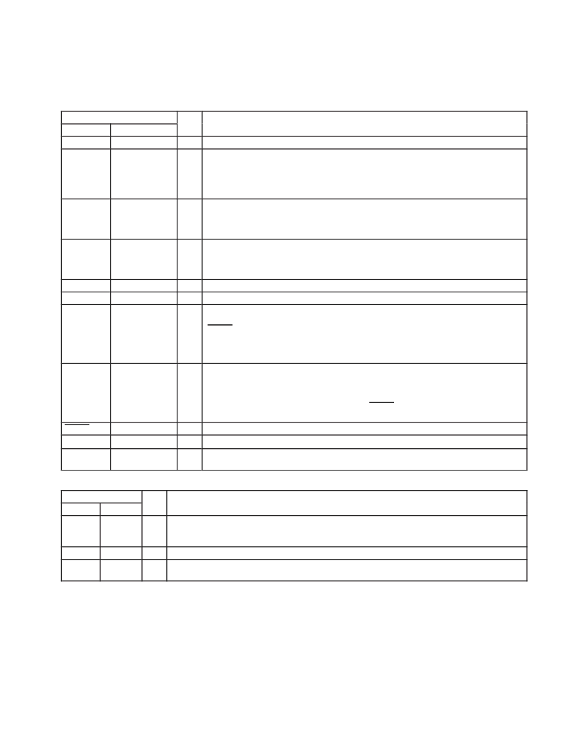
Table 24. Power Supply Terminals
TERMINAL
I/O
DESCRIPTION
NAME
NUMBER
AGND
R14, U13, U14
Analog ground terminals
AVDD
P13, P14, U15
3.3-V analog circuit power terminals. A parallel combination of high frequency decoupling capacitors
near each terminal is suggested, such as 0.1
μ
F and 0.001
μ
F. Lower frequency 10-
μ
F filtering
capacitors are also recommended. These supply terminals are separated from VDPLL_33 internal
to the controller to provide noise isolation. They must be tied to a low-impedance point on the circuit
board.
GND
F07, F10, F13,
G14, H06, K06,
K14, M14, N06,
P07, P09
Digital ground terminal
VCC
F06, F09, F12,
F14, J06, J14,
L06, L14, P06,
P08, P10
3.3-V power supply terminal for I/O and internal voltage regulator
VCCA
VCCP
A15, J19
Clamp voltage for PC Card A interface. Matches card A signaling environment, 5 V or 3.3 V
P01, W08
Clamp voltage for PCI and miscellaneous I/O, 5 V or 3.3 V
1.5-V PLL circuit power terminal. An external capacitor (0.1
μ
F recommended) must be placed
between terminals R17 and U18 (VSSPLL) when the internal voltage regulator is enabled
(VR_EN = 0 V). When the internal voltage regulator is disabled, 1.5-V must be supplied to this
terminal and a parallel combination of high frequency decoupling capacitors near the terminal is
suggested, such as 0.1
μ
F and 0.001
μ
F. Lower frequency 10-
μ
F filtering capacitors are also
recommended.
VDPLL_15
P15
VDPLL_33
U19
3.3-V PLL circuit power terminal. A parallel combination of high frequency decoupling capacitors
near the terminal is suggested, such as 0.1
μ
F and 0.001
μ
F. Lower frequency 10-
μ
F filtering
capacitors are also recommended. This supply terminal is separated from AVDD internal to the
controller to provide noise isolation. It must be tied to a low-impedance point on the circuit board.
When the internal voltage regulator is disabled (VR_EN = 3.3 V), no voltage is required to be
supplied to this terminal.
VR_EN
K02
I
Internal voltage regulator enable. Active low
VR_PORT
K01, K19
I/O
1.5-V output from the internal voltage regulator
VSPLL
R17, U18
PLL circuit ground terminal. This terminal must be tied to the low-impedance circuit board ground
plane.
Table 25. PC Card Power Switch Terminals
TERMINAL
I/O
DESCRIPTION
NAME
NUMBER
CLOCK
A09
I/O
Power switch clock. Information on the DATA line is sampled at the rising edge of CLOCK. CLOCK defaults
to an input, but can be changed to an output by using bit 27 (P2CCLK) in the system control register (offset 80h,
see Section 4.29).
DATA
B09
O
Power switch data. DATA is used to communicate socket power control information serially to the power switch.
LATCH
C09
O
Power switch latch. LATCH is asserted by the controller to indicate to the power switch that the data on the DATA
line is valid.
相關(guān)PDF資料 |
PDF描述 |
|---|---|
| PCI6420 | Integrated 2-Slot PC Card & Dedicated Flash Media Controller |
| PCI6421 | DUAL/SINGLE SOCKET CARDBUS AND ULTRAMEDIA CONTROLLER |
| PCI6611 | DUAL/SINGLE SOCKET CARDBUS AND ULTRAMEDIA CONTROLLER |
| PCI6621 | DUAL/SINGLE SOCKET CARDBUS AND ULTRAMEDIA CONTROLLER |
| PCI6515 | SINGLE SOCKET CARDBUS CONTROLLER WITH DEDICATED SMART CARD SOCKET |
相關(guān)代理商/技術(shù)參數(shù) |
參數(shù)描述 |
|---|---|
| PCI4520 | 制造商:TI 制造商全稱:Texas Instruments 功能描述:DUAL-SOCKET PC CARD AND INTEGRATED 1394A-2000 OHCI TWO-PORT PHY/LINK-LAYER CONTROLLER |
| PCI4520GHK | 功能描述:外圍驅(qū)動(dòng)器與原件 - PCI 2 Slot PC Card & int 1394a-2000 RoHS:否 制造商:PLX Technology 工作電源電壓: 最大工作溫度: 安裝風(fēng)格:SMD/SMT 封裝 / 箱體:FCBGA-1156 封裝:Tray |
| PCI4520ZHK | 制造商:Texas Instruments 功能描述: |
| PCI-471LF | 制造商:PROTECHSYSTEMS 制造商全稱:PROTECHSYSTEMS 功能描述:PCI ULV Celeron M CPU Card |
| PCI5 | 制造商:未知廠家 制造商全稱:未知廠家 功能描述:Fuse |
發(fā)布緊急采購,3分鐘左右您將得到回復(fù)。